Nanotechnologist Ralph E. Merkle (see www.merkle.com) has described current manufacturing methods as being akin to building a castle out of Lego blocks while wearing boxing gloves...
Biophysicists from Cornell University (Ithaca, NY) have joined forces with a chemist from Université de Rennes (Rennes, France) to tackle one of the biggest optical-imaging challenges...
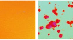
Researchers at the Georgia Institute of Technology (Georgia Tech; Atlanta, GA) are working with a local bakery to develop a machine-vision system to automatically inspect freshly...
Using technology based on a continuous-wave near-IR imager first demonstrated in 1996 by Britton Chance, emeritus faculty at University of Pennsylvania (Philadelphia, PA), and...
Two groups of researchers have advanced the use of electrowetting droplets for displays, with one demonstrating a new way of exploiting the optical geometry of the liquid used...
A fast modulator made of silicon (Si) may make researchers take another look at the material, which has been largely forsaken by the optoelectronics industry in favor of other...
"Immersion" was the word at the SPIE Microlithography 2004 meeting (Santa Clara, CA; Feb. 22–27) as chipmakers put off the tough climb to 157-nm optical lithography and opted ...
A team at the University of California–Berkeley has devised a system that can perform light-induced fluorescence spectroscopy, has an area less than 1 cm2, and is less than 1....
In a development that may one day help in the fabrication of nanometer-scale optical devices, engineers at Nippon Telegraph and Telephone Corp. (NTT: Tokyo, Japan) have created...
In a Rydberg atom (or molecule), an outer electron is excited to a high quantum state without being ionized, resulting in an atom with a very large electron cloud.
The optical output of a short-arc lamp is kept stable in the short term by good power-supply design, and in the long term by a closed-loop light-intensity control system.
Shuji Nakamura's seemingly single-handed invention of practical gallium nitride–based blue and UV lasers and light-emitting diodes (LEDs) during his stint at Nichia (Kaminaka,...
When a planet with an atmosphere passes in front of a star (an event known as an occultation), earthbound scientists can glean information about the planet's atmosphere by examining...
Rofin-Sinar acquires Swedish fiberoptics firm; IDS expands portfolio with patent on medical imaging system; Report optimistic on future of long-wavelength lasers; MORE...
Active-photonic-lattice distributed-feedback lasers emit a diffraction-limited surface-normal beam. These lasers can be coherently combined into arrays that could potentially ...
Regional phone companies in the United States have left fiber rollout to others, but as bandwidth demands increase, fiber to the home is gradually gaining momentum.
Technical sessions will reveal what is ahead in the areas of semiconductor emitters, displays, nonlinear and ultrafast optics, sensing, and biological applications.
Wavefront sensing for adaptive optics (AO) has become an essential component in building large ground-based telescopes and telescope interferometers for 21st century astronomy...
The best way to design and test coatings for use at 193 nm relies on two approaches: one for high pulse energy and low repetition rate, and the other for low pulse energy and ...