Lab on a chip is designed for the field
A team at the University of California–Berkeley has devised a system that can perform light-induced fluorescence spectroscopy, has an area less than 1 cm2, and is less than 1.5 mm thick. While the more expensive electronic part of the chip—which includes CMOS detectors, two different light-emitting diodes (LEDs), and a color filter—can be retained, researchers designed the part that carries the chemical or biological sample to be discarded after each use. Although the system itself is relatively simple, integrating the components has involved the development of new techniques, and shielding the detector is an ongoing challenge. The team hopes that the new system will eventually be of use in field situations where time is critical and taking samples back to the lab is not an option.
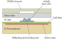
At the top of the device is a glass slide covered by a piece of polydimethylsiloxame (PDMS; see Fig. 1). The top was fabricated to include microchannels by using a molding technique that involves patterning silicon with an inverted structure using deep-reactive-ion etching and then depositing the PDMS on top. The latter can then be detached from the silicon, attached to the glass, and the resulting device used to carry liquids to be tested for chemical species and the fluorescent dye molecules they have been tagged with. When excited using LEDs located immediately underneath the microchannels, the dyes emit light at their signature wavelength. This light is picked up by the silicon photodetector beneath the light sources. The resulting intensity indicates the concentration of the chemical in question.
One of the most crucial design issues for the team was to prevent light directly emitted by the LEDs from being sensed. This is necessary to detect low concentrations of chemicals when the fluorescent signal will be very weak. In their existing system, the Berkeley researchers had two main strategies in mind. First, they designed the chip so the light sources sat between the sample and the detector, with a metal reflector and bonding pad forcing the light up. This would prevent any direct leakage to the detector. Second, they wanted to use a color filter over the detector to try to block all but the precise wavelengths of interest.
Cadmium sulfide filter
Unfortunately, geometrical restrictions imposed by the first strategy made it more difficult to implement the second. Because of the reflector, normally incident light from the sample could not reach the detector. The filter must, therefore, work for light coming in over a range of angles. Classic Bragg reflectors—layered stacks whose reflective properties are determined by the material and layer thickness—are very sensitive to input angle, the permitted wavelength increases with the angle from the normal. So the team had to find another solution, which turned out to be cadmium sulfide (CdS). This semiconductor works well as a filter, has sharp cutoff frequencies and, as it turns out, can be engineered to work with cutoff wavelengths varying from 513 to 714 nm. This is achieved by using different compositions of CdSxSe1–x in the pulsed laser deposition, in which the target is exposed to 10-Hz pulses from an excimer laser to produce the material emissions. Results for the filter used in their system were almost as good as for a commercial Bragg-reflector stack.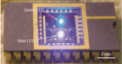
Since light emitters are difficult to grow on silicon, integrating the LEDs was another important step. For this, the team developed a technique called pixel-to-point transfer, which involves picking up an element grown on (for instance) sapphire using a pickup rod and some cyanoacrylate glue, using laser liftoff to remove the sapphire substrate (by weakening the bond between substrate and device), and then bonding to the final location with palladium and indium and removing the temporary substrate. The advantage of this kind of technique, researchers say, is that different emitters made using different materials systems can be used on the same chip; they have already demonstrated a two-LED design (see Fig. 2).
Currently, the lowest molar concentration that the device can detect is 1.2 × 10⁻⁷. Improvements may be possible by using an antireflection coating at the filter and—where the wavelengths are such that there will be no increase in crosstalk from the LED—a reflective coating to prevent fluorescently emitted photons from leaving the device.
REFERENCE
- J. Alex Chediak et al., Sensors and Actuators A 111 (March 2004).
About the Author
Sunny Bains
Contributing Editor
Sunny Bains is a contributing editor for Laser Focus World and a technical journalist based in London, England.