EV Group (EVG) targets the global semiconductor, MEMS and nanotechnology markets with its industry-leading wafer-bonding, lithography/nanoimprint lithography (NIL), metrology, photoresist coating, cleaning and inspection equipment. www.EVGroup.com
ST. FLORIAN, Austria, September 29, 2026—EV Group (EVG), a leading provider of innovative process solutions and expertise serving leading-edge and future semiconductor designs...
Comprehensive portfolio of wafer bonding and nanoimprint lithography technologies enables customers and partners to develop scalable CPO architectures for AI-driven data centers...
ST. FLORIAN, Austria, May 19, 2026—EV Group (EVG), a leading provider of innovative process solutions and expertise serving leading-edge and future semiconductor designs...
New EVG®6200 NT platform enables high-resolution, scalable fabrication of next-generation micro- and nanostructures WARSAW, Poland and ST. FLORIAN, Austria, April 21, 2026...
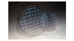
High-index glass wafers are the basis of flexible waveguide designs that bring a new generation of full-immersion augmented reality eyewear closer to fruition.
Introduced at SPIE's Photonics West 2020, the arrays of waveguide optics on high-index glass have wide field of view, aim for mass-production quantities.