From pixels to optical links: MicroLEDs pivot to copackaged optics

MicroLED has long been seen as the future of direct-view displays because of its inherent characteristics, but the manufacturing cost and yield could delay or even cancel this outlook. That said, augmented reality (AR) glasses already account for the majority of microLED volume, as brightness requirements favor the technology. It also seems that the technology has found a new market opportunity in the form of CPO.
CPO application benefits from the compound growth of both AI infrastructure and the replacement of copper transmission by photonics. It moves the optical engine—lasers, modulators, and photodetectors—from a pluggable module to a position next to the application-specific integrated circuit (ASIC), a switch chip or graphics processing unit (GPU). It shortens the electrical path, reduces power consumption, and increases bandwidth.
Wide and slow architecture
Since 2025, collaborations to integrate microLED into CPO have flourished, with almost every major player in the microLED industry involved in developing a solution. Avicena, with its LightBundle prototype, is the pioneer. It uses blue gallium nitride (GaN) microLEDs paired with silicon photodetectors provided by TSMC, instead of lasers, to move data optically. This approach trades per-channel speed for parallelism. Instead of one very fast channel, data is split across dozens of low-speed channels (3 Gbps per LED for LightBundle compared to 50 Gbps for a laser). This is the core of microLED’s value proposition and it’s often referred to as the “wide and slow” architecture, as detailed in Yole Group’s 2026 report MicroLED: Applications, Markets and Competitive Landscape.
This architecture brings a key advantage. At around 3 Gbps per channel, the signal is slow and clean enough to bypass digital signal processor (DSP) and ADC/DAC signal processing electronics and bring link-level energy consumption down to 1 pJ/bit (if SerDes is removed), compared to 5 pJ/bit for laser-based links. In its current form, LightBundle delivers 512 Gbps and scales to 896 Gbps. Microsoft has also demonstrated a prototype, MOSAIC, which distributes an 800-Gbps link across 400 channels at 2 Gbps each, in a 20 × 20 array footprint of <1 mm2.
The chips’ tiny size is a major advantage for packaging them together. Cost reductions are also to be expected with a cheaper emitter and a mature emitter/complementary metal-oxide semiconductor (CMOS) driver integration. Because they emit visible light, photodiodes (PD) for this wavelength exist and are cost-effective. Made mostly of GaN materials, they don’t rely on the indium phosphide (InP) substrate supply chain that can be under stress. Finally, the absence of thermal stabilization removes the need for external modules, which enables the CPO to sit closer to the chips than a laser-based solution can.
Scale-in: A microLED sweet spot
The incoherent nature of microLED makes it better suited to address short-distance communication. Short-distance links fall into the scale-in segment defined in Yole Group’s 2026 report Copackaged Optics for Data Centers (see Fig. 1). The bandwidth requirement for this category is expected to represent roughly 30x the combined scale-up and scale-out volume in the future.
To turn this potential into deployable products, an ecosystem is taking shape. In March 2023, Avicena signed a joint development agreement with ams OSRAM, combining LightBundle with the company's mass-production experience in microLED. Microsoft partnered with MediaTek, Credo acquired Hyperlume, and Marvell invested in Mojo Vision. Artilux’s spinoff Brillink leverages its parent company’s germanium silicon (GeSi)-based PD array technology and uses PlayNitride’s first-generation microLEDs, the same as those used in the Garmin Fenix 8 Pro and Samsung microLED TVs. Serviceability is also being addressed. At ECOC 2026, Avicena demonstrated the first connectorized version of the link. The next milestones to watch for will be manufacturing yield, thermal behavior inside the package, and the first customer qualification programs.
Three hurdles remain
Behind the industrial milestones, several technical bottlenecks remain at the device level with microLED CPO architecture. The first one is the optimization of the LED (see Fig. 2, item 1) for high modulation bandwidth without degrading efficiency. It must also run at a low enough current to be compatible with CMOS backplane drivers. As the size of the LED shrinks, current density increases and the modulation frequency rises. But one of the drawbacks of die size reduction is the reduction of EQE and, ultimately, the loss of optical power. The industry needs to concentrate its efforts on this tradeoff to exploit a high modulation bandwidth while maintaining optical power efficiency.
A second bottleneck lies in optical coupling and connectivity (see Fig. 2, item 2). Without microlenses or resonant cavities, microLEDs have a broad emission angle (~180°), while optical fibers accept light over narrow angles only (~20°). One solution could be to deposit microlens arrays during the manufacturing process to collimate the LEDs’ beams, if this monolithic integration is possible. Fiber-bundle stiffness can also be an obstacle when integrating the solution into a tiny, constrained zone.
The signal then has to be processed and integrated into the electronics (see Fig. 2, item 3). Driving hundreds of LEDs in parallel with high current density per emitter while ensuring uniformity and thermal management of the LED arrays is challenging. Hundreds of parallel signals must arrive at the receiver time-aligned, and any skew or desynchronization across the lanes would alter the signal and necessitate deskew buffers or clock forwarding, adding logic modules and latency.
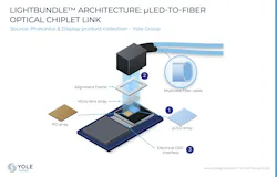
This highly parallel architecture differs from the more mature, serialized laser-and-copper-based solutions. To remain compatible with existing switch ASICs that use serial electrical input/output (I/O), a gearbox (SerDes) and drivers must be included, which partly offsets the power advantage (up to 3–6 pJ/bit). A specifically designed CMOS transceiver IC is also required to drive hundreds of channels in parallel with high current density per emitter consistently and reliably.
A new solution, not a revolution
MicroLEDs don’t offer a revolution, but are a well-founded option for CPO architectures. With no lasers, simple electronics, and silicon detectors, its advantage is real, as long as a reliable and manufacturable architecture can be delivered off the shelf. There is a certain irony in the idea that microLEDs could eventually find their place within AI infrastructure, where no one will ever look at them.
About the Author
 Elliot Bouchard
Elliot Bouchard
Elliot Bouchard is a Technology & Market analyst in Photonics and Display at Yole Group. Bouchard covers a range of photonics and display topics, including microLEDs, AR, photonic computing, and other related innovative technologies. He earned an engineering degree from Phelma–Grenoble INP (Institut National Polytechnique in France) and spent a year in the Physics Department at Imperial College London (U.K.), where his studies focused on photonics, electronics, and optoelectronics.