Silicon meets light: Photonic paths to AI-scale connectivity
Photonics technologies are playing a crucial role in data communications, particularly to address increasing demands for high-speed, high-bandwidth, and energy-efficient data transfers.
Data centers rely on multiple levels of optical interconnects for applications ranging from chip-to-chip connections (<1 meter) to data center interconnects (<100 kilometers). High-speed optical transceiver modules can accommodate various photonic devices, such as vertical-cavity surface-emitting lasers (VCSELs), external modulated lasers (EMLs), and continuous-wave distributed feedback (CW-DFB) lasers for silicon photonic integrated circuits (PICs). The specific application requirements determine which laser technology is selected.
EMLs offer clear advantages—proven stability and reliability, suitability for mid- and long-haul transmission, and high signal quality and manufacturing yields—but their power efficiency and cost are limiting at higher bandwidths. With limited room to shrink or integrate further, more devices are required per module at 1.6T and above, which drives up both power consumption and cost.
Within the rapidly evolving optical interconnects market, demand for scalable, high-speed, energy-efficient modules is surging, thanks to artificial intelligence (AI) clusters and hyperscale cloud data centers. And photonic integration is accelerating as a key enabler of miniaturization, better power efficiency, higher performance, lower cost, and scalability, as well as a platform for new functionality.
Why silicon PICs?
Silicon photonics appears to be the most promising platform for high-speed optical interconnects. Silicon PICs fabricated on silicon-on-insulator (SOI) with complementary metal-oxide semiconductor (CMOS)-compatible processes can leverage established foundry infrastructure for large-scale, cost-effective manufacturing.
PICs are specialized chips that integrate various optical components like lasers, modulators, and detectors onto a single substrate to enable the manipulation of light within a compact footprint. Cost efficiency requires material economics, integrated design, and fewer lasers.
High-density integration also reduces optical losses, and silicon photonics is often paired with indium phosphide (InP) for hybrid or heterogeneously integrated light sources. This hybrid approach is widely used at 100G/lane and is expected to extend to 200G/lane, although several challenges must be addressed to ensure a smooth transition.
To achieve 400 Gbps per lane and beyond, the industry is exploring deeper integration of new materials for modulators, detectors, and waveguides on SOI substrates. The heterogeneous integration of not only III-V lasers but also new materials adds complexity that lowers the yield results, which adds to the high cost of a PIC and may delay its time to market. It’s essential for the industry to design new PICs to meet the future bandwidth requirements and make them commercially viable.
Two strategic paths: Higher speed per lane vs. ‘slow and wide’ optics
Today, the silicon photonics market is driven by pluggable transceivers used primarily by data centers. But a second promising application is copackaged optics (CPO) for scale-out networks. It’s an alternative to face-plate pluggable switches and enables higher density, lower power, and lower cost per gigabit per second. And a third application is CPO for scale-up that optically interconnects two silicon chips or any compute architecture processing units (xPUs).
The roadmap for pluggables inclines toward increasing rate per lane, while CPO systems represent the slow and wide path. Although CPO promises ultralow power and high density, many network operators and system vendors continue to favor pluggable modules for their proven cost-effectiveness, easy front-panel access, and multivendor interoperability.
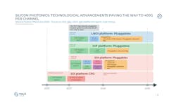
The goal: Higher speed per lane
Targeting 400 Gbps per lane enables per-port Ethernet speeds of 3.2 Tbps and beyond, while delivering roughly 20 to 30% power savings and a 50% reduction in laser count, which lowers capital expenditures (CapEx), simplifies supply chains, and reduces operating expenses (OpEx) for cooling and power delivery.
We see opportunities for several optical solutions:
- Discrete 400G EMLs will be available in high volumes for 3.2T pluggable modules.
- Silicon PICs enhanced by InP, thin-film lithium niobate (TFLN), or barium titanate (BTO) modulators, which will require mastering large-scale heterogeneous integration.
- Hybrid organic electro-optic (OEO) modulators, which can outperform TFLN/BTO-on-silicon through smaller PICs and true back-end wafer-scale finishing, although they must prove long-term stability and reliability at scale.
- Lithium niobate on insulator (LNOI) as a technology platform offers excellent electro-optic efficiency for ultrahigh-bandwidth use cases (linear pluggable optics, linear retimed optics, coherent-lite pluggables), with TFLN/LNOI suppliers developing PICs that will compete with SOI despite initial cost challenges and limited mass production.
- InP PICs stand out for monolithic integration of active photonic components, which minimize assembly complexity, but today are still a higher cost at lower production volumes.
‘Slow and wide’ optics
The yield of new materials integration on SOI platforms, as well as large-scale manufacturing of LNOI or InP platforms, may not meet the cost expectations by 2028.
Slow and wide optics hit high aggregate bandwidth by keeping each lane modest in speed while multiplying lanes across fibers or wavelengths, which eases analog design, improves signal integrity and margins, can lower per-lane power, reduce DSP complexity and latency, leverage mature, lower-cost components (especially for short reach), and often improve yield and reliability. But the approach has problems elsewhere: It requires many more serializers/deserializers (SerDes) and fibers, which strain package pins, retimers, copackaging budgets, and front-panel density. Slow and wide shines for short-reach intra-rack/row links and latency-sensitive AI/machine learning clusters using simple non-return-to-zero (NRZ)/pulse amplitude modulation (PAM) with light—ideal for CPO systems.
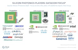
Silicon photonics industry focuses on innovation
The silicon photonics industrial landscape is forming around diverse players: Major vertically integrated players actively engaged within the silicon photonics industry, startups and design houses, light source suppliers, and foundries.
Numerous startups are focused on silicon photonics technology and aim to bring innovation to the market. These startups often focus on specific applications or novel technologies such as high-speed transceivers, optical engines for CPO, and LiDAR systems. Foundries serve as foundational partners for companies innovating in silicon photonics, offering fabrication capabilities, process development, and support for commercial production, allowing businesses to scale silicon photonics technology for diverse applications.
China closes the gap
China is making significant advancements in silicon photonics technology and aims to establish itself as a leader within the field. As it rapidly closes the gap with Western companies by leveraging government support, China is focusing on domestic innovation and scaling up production for high-speed optical communications solutions. These efforts position China as a significant contender for global silicon photonics. Although more Chinese startups are entering the silicon photonics field, local companies have full technical capability and are working to close this gap and advance higher-speed silicon photonics solutions.
Forecast: Significant growth on the horizon
As data center operators demand ever-higher bandwidth per watt and lower total cost of ownership, the battle among optical technologies—InP/TFLN/BTO/organics-on-SOI platform, traditional discrete lasers (VCSELs and EMLs), LNOI PIC, and InP PIC platforms—will intensify.
Pluggable modules, whether IM-DD or coherent-lite, will continue to evolve in speed, integration, and power efficiency. Meanwhile, CPO efforts will need to demonstrate robust performance and ease of deployment before they can replace pluggables in mainstream systems. The next five years will determine which material platform delivers the optimal balance of cost, power, and performance.
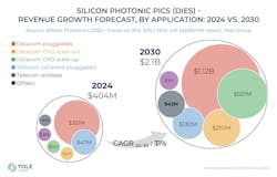
The silicon PIC (dies) market was worth $404M in 2024 and is forecast to grow to more than $2.1B in 2030 at a 31% CAGR from 2024 to 2030. This growth will be driven mainly by high-data-rate pluggable modules to increase fiber-optic network capacity. Projections of rapidly growing training dataset sizes also show that data will need light to scale machine learning models using optical input/outputs for machine learning servers.
About the Author
Martin Vallo
Martin Vallo, Ph.D., is senior technology and market analyst of photonics at Yole Group. He specializes in optical communications and semiconductor lasers within the Photonics & Sensing activities at Yole Group. With 12 years’ experience within semiconductor technology, Vallo is involved in developing technology and market products, as well as custom consulting projects. Prior to Yole Group, he worked at CEA (Grenoble, France) on the epitaxial growth of indium gallium nitride/gallium nitride core-shell nanowire light-emitting diodes by metal-organic chemical vapor deposition and their characterization for highly flexible photonic devices. Vallo graduated from Academy of Sciences, Institute of Electrical Engineering (Slovakia) with an engineering degree in III-nitride semiconductors.