Photonics are at the forefront of new microdisplay technologies
Liquid-crystal displays (LCDs) and organic light-emitting diodes (OLEDs) served us well for decades, but demand for smaller and more efficient displays for smartphones, wearables, and virtual reality (VR)/augmented reality (AR)/mixed reality (MR) headsets is now driving development of displays based on microLEDs and microOLEDs.
While microdisplay technologies provide advantages over LCDs and OLEDs, like lower power consumption, increased brightness, and a quicker response time, manufacturing challenges must be overcome before they see widespread adoption.
Market forecast for microdisplays
Thanks to microLED displays’ advantages over traditional display technologies for high-end consumer electronics, between 2024 and 2032, they’re expected to be the fastest growing display technology.1
U.K.-based Hendy Consulting, a specialist in display and semiconductor technologies, recently predicted the global microLED business will grow from $200M in 2024 to $3.6B by 2030. Key market drivers? Bright and power-efficient displays for AR/VR/MR (48%), TVs (38%), smartwatches (7%), automotive (6%), and auto head-up displays and signage (1%).
In the same report, the global microOLED business is predicted to grow from $700M in 2024 to $3.5B by 2030, driven primarily by VR and passthrough AR (79%) and smart glasses (21%).
European photonics companies address microdisplay manufacturing challenges
MicroLED technology was integrated into high-end TVs, but the production of microLED displays requires intricate fabrication techniques that are both costly and difficult to scale for mass production.
Similarly, while microOLEDs are well placed to complete with microLEDs for AR applications, they suffer from lower brightness and shorter material lifetimes because they are made of organic emissive materials. They’re also more expensive to produce and have lower yields due to organic material inconsistencies, defects from deposition, and limited scalability beyond wafer-scale fabrication.
Silicon wafer technology
To ensure scalability and cost-effectiveness, MICLEDI Microdisplays, a Belgian fabless company, uses 300-mm silicon wafer technology for high-volume production.
The process taps super-thin silicon wafers (300-mm wide) and standard complementary metal-oxide semiconductor (CMOS) fabrication techniques. Gallium nitride (GaN) is used to enhance microLED performance, and the microLEDs are bonded to a smart base (chip-like structure) to control how each LED lights up. And a microscopic lens placed on each LED at the pixel level makes the display brighter and sharper by focusing its light more effectively.
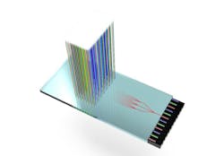
Quantum light chip
Vitrealab’s quantum light chip (QLC; see Fig. 1) is designed to enable ultraprecise light control within a photonic integrated circuit (PIC). Using direct laser writing, the company fabricates intricate three-dimensional (3D) optical networks to guide light, which is key for AR glasses, where it delivers bright, high-contrast images.
By leveraging 3D waveguide architectures, they overcome traditional planar limitations to enable ultracompact and lightweight display solutions. Vitrealab’s innovation paves the way for the next generation of AR displays—redefining visual experiences with cutting-edge integrated optics.
Advanced laser-based solutions
Another microdisplay fabrication challenge is precise and efficient transfer of microLEDs onto display substrates. Coherent has developed laser-based solutions, such as laser lift-off (LLO) and laser-induced forward transfer (LIFT), for accurate positioning of microLEDs to enhance production efficiency and yield.
An essential item is a high-performance backplane, which requires precise material processing. Coherent’s excimer laser annealing process transforms amorphous silicon into low-temperature polycrystalline silicon, and this conversion enhances the electronic properties of display backplanes to enable brighter, higher-resolution, and more energy-efficient screens.
Substrates
Many microLEDs rely on GaN to generate light because the material emits light efficiently across a wide range of wavelengths. But producing microLEDs with dimensions as small as 1 µm requires advanced fabrication techniques to achieve the necessary high precision and uniformity. German company QubeDot specializes in processing GaN to enable such diminutive light sources.
QubeDot developed a structured micro-illumination light engine (SMILE) platform to offer customizable microLED arrays with varying pixel counts, sizes, wavelengths, and intensities for biology, optogenetics, microscopy, and process metrology applications.
Photomasks
Photomasks are critical for the production of microLED displays, because they enable precise patterning of microLED chips on semiconductor wafers. A photoresist layer is first applied to the wafer and exposed through the photomask using deep ultraviolet (DUV) light. Exposed areas are then removed (negative resist) or retained (positive resist) to create microLED structures such as active regions (where light is emitted), contacts, and electrodes for electrical connections. Photomask-based alignment ensures accurate positioning for mass transfer of the LEDs onto a display backplane.
In September 2022, Japan-based Toppan Photomask (now Tekscend Photomask) partnered with EV Group, an Austrian supplier of semiconductor manufacturing equipment and process solutions to promote nanoimprint lithography (NIL) as a high-volume manufacturing process for the photonics industry for AR and VR headsets, smartphone sensors, and automotive imaging systems.
Adhesives
German high-tech adhesives manufacturer DELO is actively advancing microdisplay technology by developing specialized adhesives for microLED applications (see Fig. 2). Recognizing the limitations of traditional soldering methods, particularly the risk of electrical short circuits as LED components continue to shrink in size, the company explored the use of adhesives to connect microLEDs to the display backplane.
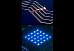
In a feasibility study using directional conductive adhesives to connect miniLED dice, results showed reliable bonding strength and high yields—both electrically and mechanically—during on-light testing. Adhesives enhance the manufacturability of miniLED displays, which paves the way for large-scale production of microLED displays for next-generation consumer and automotive applications.
Advanced OLED-on-silicon microdisplay technologies (microOLEDs)
Standard OLED displays use glass or plastic substrates, but for OLED-on-silicon technology the OLEDs are integrated directly onto a silicon substrate. It leverages the benefits of OLEDs and silicon-based electronics to enable smaller pixel sizes and higher pixel densities for compact, high-performance microOLEDs, which are used for near-eye applications such as AR and VR devices, head-mounted displays, and viewfinders.
Fraunhofer Institute for Photonic Microsystems (IPMS) is at the forefront of this technology. Traditional silicon-based microdisplays lack transparency, which limits their use for AR systems. As a solution, Fraunhofer IPMS developed semitransparent OLED-on-silicon microdisplays that achieve up to 45% transparency to enable ultralight, compact AR systems.
CEA-Leti is also playing a key role in microdisplay development. Leveraging its expertise through a longstanding collaboration with French company Microoled, CEA-Leti is advancing OLED microdisplays with enhanced color accuracy and improved energy efficiency for near-eye applications. They’ve also pioneered GaN-based microLED display technology, which opens the door for new AR/MR applications (see Fig. 3).
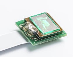
This technology presents significant challenges, which CEA-Leti is addressing by enhancing color generation through advanced native RGB growth techniques or color conversion solutions, combined with integration technologies to seamlessly connect high-resolution, small-pitch GaN arrays with CMOS circuits.
Advanced measurement instruments for display technologies
Advanced measurement instruments are crucial to ensure quality, efficiency, and precision at every stage of the microdisplay manufacturing process. Dutch company Admesy’s high-end spectrometers and colorimeters offer precise measurements, while their imaging colorimeters offer high spatial resolution and speed, which are crucial to assess luminance and color uniformity.
Italy-based Alfamation provides advanced test systems for the display sector. Their automated display tester is designed for automotive displays, instrument clusters, and components such as microlenses, diffractive optical elements, meta-optical elements, and microlens arrays.
Germany-based Instrument Systems also provides state-of-the-art metrology solutions for research labs and high-volume production of microLED and microOLED microdisplays and wafers. Their innovative concept integrates a high-speed camera and high-resolution optics with a precise spectrometer for traceable spectral referencing. It ensures sub-micron-level quality control for microLED display products and measurements of electroluminescence and photoluminescence.
Future outlook
Manufacturing challenges remain, but the future looks bright for the microdisplay industry. Advantages microLEDs and microOLEDs provide over traditional display technologies make them ideal for many applications. As manufacturing processes improve and costs decline, we expect widespread adoption of microdisplays across industries—from consumer electronics to automotive and beyond.
Photonics is not merely an enabling technology but sits at the very core of the microdisplay revolution. The remaining hurdles—mass-manufacturing scalability, cost reduction, and efficiency improvements—are immense opportunities for the photonics sector.
Continued innovation in areas such as high-throughput laser systems, novel PIC architectures, advanced optical materials, efficient light-extraction techniques, and rapid high-resolution measurement solutions will be crucial. For the photonics community, driving progress in microdisplays is about reaffirming the fundamental role of the science of light and technology in shaping future human-machine interfaces and advancing frontiers. Collaboration across the ecosystem—from materials scientists and device engineers to systems integrators—will be key to unlocking this bright future.
REFERENCE
About the Author
Jérémy Picot-Clémente
Jérémy Picot-Clémente is photonics technologies manager for the European Photonics Industry Consortium (EPIC), and is based in Auvergne-Rhône-Alpes, France.