Waveguide optics: Going beyond classical fiber optics
Waveguide optics are much more than the classical solid-glass optical fiber drawn into a circular cross-section by the surface tension of molten glass. Waveguide optics include the planar waveguides in the active layers of diode lasers, and the many types of planar waveguides that transport light and serve as couplers, ring resonators, and other components in integrated photonic chips. Waveguide optics can even put the Nobel-winning laser frequency comb onto a photonic chip.
The roots of waveguide optics go back to James Clerk Maxwell’s theory of electromagnetic radiation. Lord Rayleigh developed the first mathematical waveguide theory in 1897 for hollow metal cylinders, and the study of nonconductive dielectric waveguides followed. The theory was developed for electromagnetic waves in general, was tested on radio waves, and also has been shown to describe total internal reflection in optical fibers and light guiding in planar waveguides.
Modal effects
Waveguide theory describes the propagation of light and other electromagnetic waves, including mode patterns. Centimeter-scale rectangular metal waveguides worked well for microwave signals of about the same size. Propagation modes did not become important until the mid-20th century when radio frequencies increased to tens of gigahertz, where many waves could fit inside a waveguide. In the 1950s, designers of 5 cm “millimeter waveguides” to transmit telephone traffic did not realize how much trouble multimode transmission would cause when they tried to transmit 60 GHz (0.5 mm) signals through long lengths of this buried waveguide.
Modal effects emerged in fiber optics a few years after they were developed in the 1950s based on total internal reflection. Developers trying to improve resolution for medical applications by shrinking fiber cores to micrometer size were surprised to see odd light patterns in the fibers. Elias Snitzer at American Optics (Southbridge, MA) recognized the patterns as single-mode transmission. Charles Kao, who had worked on the millimeter waveguide, suggested single-mode transmission through optical fibers to avoid the problems of multimode transmission in the millimeter waveguide, although single-mode fiber was not widely adopted until the 1980s.
Waveguide theory also revealed that total internal reflection was not total. Instead, an evanescent wave extended from the high-index core into the low-index cladding, declining exponentially in intensity. Like modes, this also has important consequences when sizes are on the order of the wavelength.
Planar waveguides and integrated optics
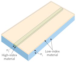
In 1969, Stewart E. Miller of Bell Labs proposed developing monolithic “integrated optics,” with light carried by simple high-index planar glass waveguides as narrow as 2 µm embedded in a lower-index cladding (see Fig. 1). Calculations showed that evanescent waves could leak between two closely spaced parallel waveguides, optically coupling light between them. Other early ideas included making silicon waveguides surrounded by silica or air and making modulators by diffusing titanium into lithium niobate waveguides.
Planar waveguides soon found a home in diode lasers. Their rectangular cross-section is compatible with photolithography and semiconductor fabrication techniques used in double heterostructures, in which the high-index active layer is sandwiched between two lower-index layers. The widely used stripe geometry used in diode lasers is a planar waveguide a fraction of a micrometer thick and only a few micrometers wide.
Progress in integrated photonics as a whole has been much slower. Photons in the optical range are larger than electrons and their interactions with each other via matter generally are weaker than for electrons, so integrated-photonic components tend to dwarf transistors. But broad progress has been made in overcoming those limits.
Materials for integrated photonics
Silicon is the leading material for integrated photonics, because it has a tremendous industrial base and can provide electronic components vital for photonics. It is transparent from 1100 to 3500 nm, spanning the 1310 and 1550 nm windows, and its high refractive index in that range—about 3.5—allows it to guide light around strong curves in small components. Its biggest weakness is its indirect bandgap, preventing it from generating light efficiently for lasers. In practice, light-emitting III-V semiconductors, usually with indium phosphate (InP) substrates, are flip-chip bonded to the silicon base, making silicon integrated-photonic hybrids.
Integrated photonics also can be based on InP, which is transparent from 1000 to 2500 nm, covering the key fiber windows. InP has a direct bandgap, and III-V semiconductors can be grown on it to make lasers, detectors, and other components. It is used commercially for high-performance communications transmitters and receivers, but the industrial base is much smaller than silicon and the costs are higher.
Silicon dioxide (SiO2) and some other glasses are also attractive because they are transparent from 300 to 2500 nm, and their attenuation in waveguides is much lower than the decibels per centimeter of most other waveguide materials. However, the refractive index of SiO2 is 1.45, preventing it from confining light as strongly as silicon or other high-index semiconductors. It also can’t be formed into lasers, modulators, or detectors.
Silicon nitride (Si3N4) is a relative newcomer transparent between 400 and 2350 nm, with refractive index close to 2 across that range. It usually is a thin film deposited on silica, which serves as a cladding. Quix (Enschede, Netherlands), which is developing an integrated photonic quantum processor, says its silica-clad waveguides have an attenuation of 0.001 to 0.1 dB/cm. Ligentec (Geneva, Switzerland) is integrating Si3N4 components including spirals, filters, ring resonators, Mach-Zehnder interferometers, and heaters. The company says its waveguides are usable in the 2–3 µm band.
Polymer optical waveguides have been around for many years, and Laser Focus World ran an article about how they could be used with integrated optics back in 2000. In a process called the “Mosquito method,” a cladding layer is applied in liquid form to a substrate, then a higher-index material is injected into the cladding layer, and the composite is cured under ultraviolet light to form a circular core. The process can produce multimode and single-mode cores, which can be fabricated in parallel to form a multichannel waveguide.
No known materials offer all the features sought in integrated photonics, so the quest for new ones continues. Atomic-layer deposition can form waveguides of alumina (Al2O3) on silica or silicon with losses below 3 dB/cm in the violet and near-ultraviolet, an order of magnitude less than other waveguides in that band. Silicon-germanium (Si0.2Ge0.8) Mach-Zehnder interferometers made of waveguides fabricated on a graded Si1-xGex substrate have demonstrated extinction ratios higher than 10 dB in the 3 µm band. Photodetectors of molybdenum sulfide (MoS2), a graphene-like planar material, have been integrated into silicon nitride chips.
Integrated-photonic devices
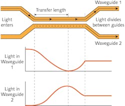
Combinations of planar waveguides can serve many functions. A simple Y coupler divides light equally between two waveguides offset at equal angles (see Fig. 2). Waveguides can be configured to form Mach-Zehnder interferometers to serve many purposes.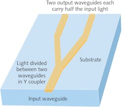
Arrayed-waveguide gratings
Combining many waveguides can produce complex effects, such as the demultiplexing of signals transmitted in dense wavelength-division multiplexing (DWDM) by the arrayed waveguide grating (AWG), one of the first planar waveguide devices to become a successful product.
As shown in Figure 4, the input signal to be demultiplexed is spread out into a broad mixing region where it couples into many parallel waveguides, each of which collects signals at all wavelengths. Lengths of the adjacent waveguides differ by an increment Δ, which delays light passing through two adjacent wavelengths by a phase shift of nΔ/λ, where n is the refractive index and λ is the wavelength. When the light emerges from the waveguides, diffraction and refraction spread it through the second mixing region, sorting the wavelengths into separate output waveguides. The actual number of waveguides linking the two mixing regions is larger than the number of wavelengths in the signal. For example, an AWG demultiplexing 64 optical channels may include 232 parallel waveguides linking the mixing regions.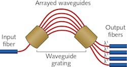
Arrayed-waveguide gratings can be used in other ways as well, such as adding or dropping optical channels at optical switches or rearranging wavelengths among input and output fibers. Some early versions were made from plastic, but today the major types include silica on silicon, which is passive, and InP, which is active and can incorporate switches and other components, but has higher attenuation, coupling loss, and crosstalk than silica.
Ring resonators
One of the most important planar-waveguide configurations is the ring resonator. In simplest form, it is a circular waveguide placed close to a linear waveguide (see Fig. 5). The linear waveguide at left serves as an input and output. Where the linear and ring waveguides are closest, evanescent waves in the linear waveguide transfer light to the ring. How much light is coupled depends on the distance between the waveguides, their structures, and details such as waveguide dimensions and refractive indices of the materials. The light is trapped in the ring waveguide by total internal reflection, except at places where other waveguides come close enough for evanescent waves to leak out into the other waveguide.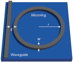
Resonances occur in the ring at wavelengths where an integral number of waves equal the circumference of the ring. That allows ring resonators to serve as filters that select what wavelengths to transfer to additional rings and/or linear waveguides. The selected wavelengths can be tuned by thermo-optic or electro-optic effects. The full range of switching and other functions possible with ring resonators is beyond the scope of this article, but, in a representative example, nonlinear effects in simple ring resonators can be used for optical switching.
Using nonlinear optics for wavelength conversion in waveguide optics is generating considerable interest, but many applications require improving efficiency. Much work has gone into third-order effects such as four-wave mixing, but others are looking at second-order nonlinearities, which can be more efficient at some power levels. A recent study showed that all-optical poling of silicon nitride waveguides could generate broadly tunable second harmonics.
Outlook
To realize how far integrated photonics has come, consider the successful demonstration of frequency-comb generators on photonic integrated circuits. Frequency combs are elegant examples of the power of modern photonics in converting ultrashort pulses into a series of uniformly spaced spectral lines of continuous light. At first, the technology behind them seemed dauntingly complex, but several years ago, intriguing proposals for microcombs surfaced.
At first, such proposals required complex modulation of both frequency and power. Earlier this year, a large group led by John Bowers of the University of California (Santa Barbara, CA), Kerry Vahala of the California Institute of Technology (Pasadena, CA), and Tobias Kippenberg of the Ecole Polytechnique Fédérale de Lausanne (Switzerland) demonstrated what they called “integrated turnkey soliton microcombs.” This device is a big step toward making a tremendously powerful and complex technology readily accessible for applications such as sensing and metrology. Waveguide optics are coming of age.
About the Author

Jeff Hecht
Contributing Editor
Jeff Hecht is a regular contributing editor to Laser Focus World and has been covering the laser industry for 35 years. A prolific book author, Jeff's published works include “Understanding Fiber Optics,” “Understanding Lasers,” “The Laser Guidebook,” and “Beam Weapons: The Next Arms Race.” He also has written books on the histories of lasers and fiber optics, including “City of Light: The Story of Fiber Optics,” and “Beam: The Race to Make the Laser.” Find out more at jeffhecht.com.