Polymer-based optical waveguide devices speed connections
RAY T. CHEN, BING LI, JAMES J. FOSHEE, WALTER B. HARTMAN, and SUNING TANG
Progress in developing optoelectronic integrated devices based on materials such as lithium niobate and gallium arsenide is impeded by several technology-related issues. Particularly daunting are the high cost of fabricating and processing related microstructures, their high refractive index and dispersion, and the need to lattice-match the substrates. These issues limit the degree of integration possible, especially on large-scale optical interconnect systems.
Polymer-based optical waveguide devices provide an alternative approach for realizing the next generation of optoelectronic integrated circuits (OEICs). These devices are hybrids that can be integrated on any existing electronic substrate. Optical polymers are formed by combining a variety of monomers into many different configurations. Several promising polymer materials with acceptable optical and mechanical properties have been developed, and many passive and active devices have been demonstrated.
The advantages of using a polymer to develop OEICs include cost-effective fabrication based on well-established technologies from the microelectronics industries. In addition, a polymer can possess combinations of electro-optic nonlinearity, photosensitivity, and thermo-optical properties. These properties make it possible to build large-size, multifunctional OEICs for the next generation of optoelectronics systems.
Fabricating a waveguide
Polymer waveguides are formed by spin-coating a polymer solution onto a substrate, forming a circuit pattern by lithography or direct laser writing, and then spin-coating another polymer layer on top for planarization. By controlling the polymer/solvent ratio and the spin speed of film coating, film thickness can be obtained in the range from 0.1 to 100 µm.
A variety of dopants can be added to the polymer film to obtain multiple functionality, such as photosensitivity and/or electro-optical nonlinearity. The photosensitivity of polymers can be used to form the multiplexed transmission waveguide hologram (grating or lens) that is crucial for building many passive and active waveguide devices.
A special poling process is often needed after spin-coating the polymer to produce the electro-optic response for fabricating high-speed electro-optic modulators. After the waveguide pattern is formed by lithography or direct laser writing, another optical polymer layer can be spin-coated again as the upper cladding film. The cladding layers can be different materials, and other functions can be introduced.
Propagation loss of less than 0.1 dB/cm of the polymer optical waveguide working at 850, 1310, and 1550 nm, respectively, has been successfully demonstrated.1-3 Important polymers include photolime gel, polyacrylates, polyimides, and polymethyl methacrylate (PMMA). These materials offer very high contrast response and latitude in the patterning process. Many optical waveguide structures have been developed, including large-scale waveguide arrays, waveguide bends, splitters, waveguide grating, and directional couplers.
Optical interconnect circuits
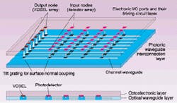
Polymer planar and channel waveguides can be easily formed on almost any type of substrate. The fabrication process is CMOS-compatible, which allows fabrication of OEICs and devices on optoelectronic substrates, so the layered hybrid integrated circuits for optical interconnection systems and photonic signal processing can be formed. Tilted gratings fabricated by holographic recording or lithography are used to realize the optical surface-normal coupling required in such circuits (see Fig. 1).
Architecturally, the conventional electronic interconnection board for ICs is replaced by a two-layer optoelectronic board. With this OEIC, gigabit-per-second system boards for computers and backplanes can be produced with no electromagnetic interference, low power consumption, and super-wide bandwidth. The topological structure design of the interconnection circuits can be very flexible, owing to the excellent features of polymer optical waveguides (see Fig. 2).4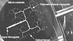
High-speed EO modulator
High-speed, electro-optical (EO) modulators require a velocity match between the guided optical wave and modulating electrical base-band signal (frequency from dc to microwave). An EO polymer waveguide has an inherent advantage in this application compared to LiNbO3 or some other semiconductor materials. The nonlinearity λ33 of 75 pm/V has been achieved in an EO polymer by an electrical poling process.5 More important, EO polymers have a low dielectric constant and very low microwave dispersion, so it is easier for a polymer waveguide modulator to reach the velocity match required by high-speed operation.
An EO modulator with a Y-branch domain-inverted waveguide-directional-coupler structure also has been demonstrated. The voltage crossing the traveling-wave electrode determines the phase mismatch between the propagation constant of channel 1 and channel 2 and, hence, the output power ratio between the two ports.
There are two poling sections in the waveguide coupler, with reversed direction, so the same cross voltage will generate the reverse phase-mismatch but at the same amplitude. It improves the linearity and efficiency of the modulator and relaxes the fabrication tolerance requirement encountered at the conventional Y-branch waveguide-directional coupler modulator. A linear waveguide modulator with a switch voltage as low as 3.6 V and an extinction ratio of 26 dB has been built in the laboratory.6, 7
Integrated laser beam deflector
Nonmechanical laser-beam deflecting and steering are of great interest because of demanding military and commercial applications such as laser tracking and targeting, laser display and printing, optical switching in fiberoptic communications, and free-space laser steering for laser communications. In an all-optical network, laser beam steering offers a novel scheme for the 1 x N switching that is a cornerstone in optical crossconnects.
The electro-optical polymer planar waveguide provides a unique opportunity to realize laser-beam deflecting and scanning in one compact OEIC. The main idea is to form a series of dynamic thin-film prisms within the planar waveguide using the EO nonlinearity of the polymer. When light passes through this series of prisms, the deflected angle will be induced by the applied voltage to the prism electrodes. Because of the thin-film nature of the devices, only low drive voltages are required.
Compared to bulky EO crystal beam deflectors, this integrated laser-beam deflector is much more compact and consumes less power. In the demonstrated device, the total thickness of three layers of waveguide is around 4 µm, the polymeric materials after poling have about 30 pm/V λ33, and 100% deflecting efficiency has been obtained. A ±1°/20-V scan ability has been observed.8 Similar devices have been demonstrated based on a thermo-optic effect in thin-film polymeric waveguides.9
WDM waveguide hologram device
The excellent photosensitive property of polymer makes it suitable for hologram recording. Thus, a novel class of waveguide hologram devices can be designed and fabricated based on planar or channel waveguides. A waveguide hologram-grating device is applicable to wavelength-division-multiplexing (WDM) applications.
The fabrication process of a waveguide hologram grating uses a two-beam interference recording method (see Fig. 3). In a simple add/drop demultiplexer (ADM), the modulation index and the reactive length of the grating can produce 100% diffraction efficiency for the desired wavelength. The wavelength that is diffracted will be determined by the grating period L, which is controlled by the recording angle between the two recording beams. A full demultiplexer for all wavelengths can be realized by cascading such units with different grating periods.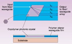
One of the most important advantages of using a polymer planar or channel waveguide grating is that the grating can have a very large two-dimensional (2-D) size. As a result, the uncertainty of the grating vector is much smaller than that of typical fiber gratings. In fact, the diffraction bandwidth of the grating can be narrow enough for dense WDM applications, while at the same time, signals at other wavelengths will not suffer scattering loss when they pass by the demultiplexer unit for a particular wavelength. Moreover, the 2-D planar structure of the waveguide circuit gives additional freedom in device design. For example, a circulator will no longer be required and the signal can be processed in parallel.
Because of the high index modulation that can be induced by photoexposure, multiplexed hologram gratings can be printed in one common space.10 Consequently, several wavelengths can be dropped off at one stage and the ADM itself is more compact, which is critical in dense WDM systems with hundreds of wavelength channels.
Photonic crystal superprism waveguide
A simple integrated WDM demultiplexer circuit can be fabricated from a quadrilateral 2-D photonic crystal dispersion element. This integrated optical demultiplexer reduces component size by hundreds of times compared to the conventional devices. Meanwhile, there is no restriction on the free-spectral range caused by the high-order diffraction in the demultiplexer based on a conventional grating.
Photonic crystals have very large dispersion characteristics (500 times that of a regular prism), which makes them very attractive for WDM applications. A "superprism" phenomenon has been observed and studied in photonic crystals.11 Using polymer waveguide technology and block copolymer photonic bandgap materials, it is possible to fabricate a waveguide superprism within polymeric planar waveguide circuits. New optical devices and the miniaturization of current integrated optical devices may result.12
ACKNOWLEDGMENT
This research is supported by the US Ballistic Missile Defense Organization, the Air Force Research Laboratory, Air Force Office of Scientific Research, NASA, Office of Naval Research, Raychem Corp., and the 3M Foundation.
REFERENCES
- T. Chen, Optics & Laser Technology 25(6), 347 (1993).
- L. Eldada et al., IEEE J. Selected Topics in Quantum Electronics 6(1), 54 (2000).
- S. Tang et al., IEEE Circuits and Devices 16(1), 10 (2000).
- R. T. Chen et al., Proc. SPIE 3632, 22 (1999).
- Y. Shi et al., Science 288, 119 (2000).
- S. Tang et al., Opt. Engineer., 39(3), 680 (2000).
- D. An et al., Appl. Phys. Lett. 76(15), 1972 (2000).
- S. Tang et al., Proc. SPIE 3949, 27 (2000).
- S. Tang et al., Appl. Phys. Lett. 76(15) (2000).
- R. T. Chen at al., J. Lightwave Technology 10(7), 888 (1992).
- H. Kosaka et al., J. Lightwave Technology 17(11), 2032 (1999).
- S. Tang, BMDO funded SBIR proposal, BMDO00-014, Electronic Materials, 2000.
Ray T. Chen is a Temple-endowed professor in electrical engineering and Bing Li is a postdoctoral fellow at the Microelectronics Research Center, University of Texas at Austin, PRC-MER, Mail Code R8600, Austin, TX 78758; e-mail: [email protected]. James J. Foshee is program director and Walter B. Hartman is supervisor, at AFRL/IFGD, Wright Patterson AFB OH. Suning Tang is chief scientist at Radiant Research, Austin, TX.