Technology Review: Laser Focus World’s top 20 photonics technology picks for 2019
When human beings approach a physics, engineering, or other technical problem, they have traditionally been happiest when they could develop an analytic solution (in the form of mathematical equations), as the ability to understand and predict via mathematics is an indication of how well both the problem and solution are understood. Einstein’s theory of general relativity is just one successful example of this approach. Of course, many problems are either only partially or not at all soluble in this way, and thus fitting curves to experimental data and other empirical approaches are essential. But, overall, the effort is to develop a human understanding of the problem at a deep level.
An utterly different problem-solving approach that has been brewing in labs for years is now making its way to the commercial world: artificial intelligence (AI), which includes the subsets of machine learning and deep learning. In AI, subtle systemic data patterns and correlations that are not understood or even grasped by humans are detected by computer algorithms and linked to desirable or undesirable outputs. By relying on the computer to control the system based on these subtle patterns, humans can get their desired results.
Sounds good, right? The only drawback—and some may not consider it much of a drawback—is that, at some levels, those humans running the show now don’t have a clue what’s going on. But AI is showing so much promise that, in increasingly complex form, it is being integrated into technical and consumer arenas. Laser Focus World headlines from 2019, including the following, illustrate this: "AI to predict rogue waves in fiber-optics nonlinear instabilities"; "FLIR invests in CVEDIA to expand AI expertise for autonomous sensing"; "AI-propelled facial recognition still has technology and legal challenges"; "Deep learning brings a new dimension to machine vision"; and "NVIDIA to acquire Mellanox to advance AI and datacenter computing solutions."
Of the 20 top Laser Focus World articles selected for this year’s Tech Review, only a couple are directly related to AI. However, optics and photonics specialists in academia, industry, and government will be both using and finding new uses for AI in the following years, greatly expanding their ability to obtain practical results from large and arcane sets of data.
The leading edge
1. and 2. Silicon photonics is under intense development to make it more practical, in particular for communications, but for other uses as well. Achievements this past year have been many, including a milestone for manufacturability, in which researchers led by a group at the Massachusetts Institute of Technology (MIT; Cambridge, MA) developed a technique for assembling on-chip photonics and electronics separately, thus enabling the use of more modern CMOS manufacturing processes for the electronics (which previously had to be made with an older, optics-compatible process). (See “Silicon photonics fabrication now uses latest CMOS process,” June 2018 issue; http://bit.ly/2019TechRev1.) And an entirely silicon-based on-chip optical link, containing an avalanche-mode LED and single-photon avalanche diode, that can be made with standard CMOS technology and embedded in an electronic chip was created by a group at the University of Twente (Enschede, Netherlands). (See “On-chip optical link is created on electronic chip for the first time,” February 2019 issue; http://bit.ly/2019TechRev2.)
3. The use of AI in imaging is being advanced by Leica (Wetzlar, Germany), which launched its Thunder microscope imager series that uses so-called “computational clearing” to eliminate out-of-focus blur when using camera-based fluorescence microscopes. The company is also developing what it calls a Personal Automated Lab Assistant (PAULA) that can analyze imagery captured by continuous monitoring of a specimen and automate a response when there are changes. Leica recently sponsored a competition to sort images of vertebrate-cell proteins using AI into different classes based on their organelles. (See “AI opens a new era in scientific imaging,” September 2019 issue; http://bit.ly/2019TechRev3.)
4. Extreme-ultraviolet (EUV) lithography for making advanced computer chips is coming into its own, with the one commercial outfit that has a product—ASML (Veldhoven, Netherlands)—having shipped numerous EUV scanners this year. The 13.5 nm light sources for the massive scanners are provided by Cymer, which is owned by ASML; Cymer’s light source uses a 40 kW CO2 laser from Trumpf (Ditzingen, Germany) to turn droplets of tin into 13.5-nm-emitting plasma. Zeiss (Oberkochen, Germany) makes the reflecting optics for these machines; the large mirrors have a surface roughness better than 0.1 nm (see Fig. 1). (See “EUV lithography revisited,” Laser Focus World online [Aug. 29, 2019]; http://bit.ly/2019TechRev4.)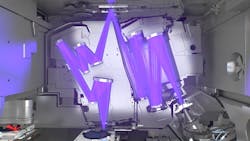
Bioscience and medical
7 The Ebola virus is deadly and highly contagious—for effective control, the earlier it is detected, the better. Scientists at the Rochester Institute of Technology (RIT; Rochester, NY) have developed a small, portable fluorescence-based instrument to rapidly detect Ebola in the field. A droplet of blood is analyzed via a continuous-wave 488 nm laser and a parabolic-mirror-based fluorometer integrated with a microfluidic chip, resulting in a sensitivity comparable to that of a confocal microscope. The test takes 15 minutes starting from the raw blood sample. The device can screen 24 subjects in parallel and process 24 samples within 30 minutes. The researchers are working on a similar instrument that detects multiple virus strains—for example, from Ebola to influenza and Zika. (See “Optical device leverages CRISPR-Cas13a technology for early Ebola detection,” June 2019 issue; http://bit.ly/2019TechRev7.)
8 While many DNA-analysis methods require a process called DNA amplification, in which a minute sample of DNA is reproduced many times to increase the sample size, a tip-enhanced Raman spectroscopy (TERS) technique developed by researchers from Texas A&M University (College Station, TX), Rensselaer Polytechnic Institute (Troy, NY), Friedrich-Schiller-Universität Jena (Jena, Germany), and Baylor University (Waco, TX) can analyze even single strands of DNA, no amplification required. The room-temperature TERS method relies on surface plasmon effects in noble-metal probe tips—when the plasmon is resonant with the excitation wavelength, intensities near the tip are greatly enhanced, increasing Raman scattering and overcoming the diffraction limit. Sequencing the DNA takes four seconds per base. (See “TERS images single-stranded DNA without amplification,” March 2019 issue; http://bit.ly/2019TechRev8.)
9 Optical coherence tomography (OCT) is improving, based on advances in photonics, computing power, and yes, AI. Via algorithms, computational OCT addresses problems that degrade the resolution of traditional OCT, including the inherent tradeoff between depth-of-field and transverse resolution, the dispersion mismatch of sample and reference paths, and aberrations imposed by optics. Machine learning has been used, for example, in OCT tissue analysis and to classify damage to human skin inflicted by burns with 90% specificity and 91.6% sensitivity. (See “Innovations in OCT,” March 2019 issue; http://bit.ly/2019TechRev9.)
10 Biosensing for detection of disease, toxins, and pathogens has been given a boost by the development of a novel class of fluorescing biological nanomaterials called DNA-stabilized metal quantum clusters (QC-DNAs) that serve as quantum biosensors. The biosensors consist of a short DNA sequence that encloses a group of six to 15 metal atoms (a so-called metal cluster). The choice of DNA sequence determines the characteristics of the sensor—for instance, which disease it is able to detect. The partners in Project BioSensing, a collaboration among two of Germany’s Fraunhofer institutes and Leiden University’s Institute of Physics (Leiden, Netherlands), are designing numerous quantum biosensors, which they plan to scale up and prepare for feasibility studies in university hospitals. (See “Quantum technology promises better biosensors,” September 2019 issue; http://bit.ly/2019TechRev10.)
11 Robotic surgery can be made more effective with the use of fluorescence techniques to, for example, distinguish between benign and cancerous tissue. Now, time-resolved fluorescence spectroscopy and imaging, which are label-free, have demonstrated capability for multiple clinical applications, as shown by a new robotic surgery study in humans. Many biomolecules in the body generate autofluorescence, and the span of time between absorption of a photon and subsequent emission is characteristic for every molecule, allowing identification. Working with time-resolved fluorescence researcher Laura Marcu of the University of California Davis (Davis, CA), robotic-surgery company Intuitive Surgical (Sunnyvale, CA) recently undertook the first-in-human study involving integration of autofluorescence in robotic oral-cancer surgery, showing its effectiveness. (See “Clinical application of time-resolved fluorescence,” April 2019 issue; http://bit.ly/2019TechRev11.)
12 Researchers at the National Cancer Institute/National Institutes of Health (NIH; Bethesda, MD) discovered a new dye (IRDye700DX) that is highly lethal to cancer cells when conjugated to an antibody, allowing near-infrared (near-IR) photoimmunotherapy. The patented technique has been licensed by the NIH to Rakuten Medical, a startup that has received Fast Track designation by the FDA for a Phase 3 trial to evaluate the therapy to treat recurrent head and neck squamous cell carcinomas. (See “NIH licenses cancer-killing near-IR photoimmunotherapy to startup,” April 2019 issue; http://bit.ly/2019TechRev12.)
Optics and photonics in practice
13 Laser ignition (LI) in automotive gasoline engines is an idea that has been pursued for years, but without reaching performance levels high enough or size small enough to get automobile manufacturers excited. Now, researchers from the National Institute for Laser, Plasma and Radiation Physics (Ma˘gurele, Romania); Renault Technologie Roumanie (Voluntari, Romania); and the University Politehnica of Bucharest (Bucharest, Romania) have drawn closer to that point with their demonstration of a LI system using fiber-coupled compact neodymium- and chromium-yttrium-aluminum-garnet (Nd:YAG/Cr4+:YAG) laser spark plugs (see Fig. 4). Laser pulses at a 1.06 μm wavelength were delivered with 4 mJ energy and about 0.8 ns duration through a sapphire window into the cylinders raised engine brake power and lowered carbon monoxide emissions in comparison to conventional spark plugs. (See “Laser ignition quantitatively improves performance of gasoline engines,” May 2019 issue; http://bit.ly/2019TechRev13.)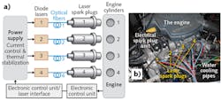
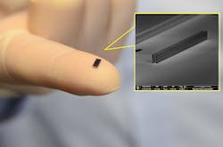
14. Spectrometers for smartphones have also been the object of much research, as such a small, portable spectrometer could be used for science in the field, or even, if simple, cheap, and effective enough, by consumers scrutinizing their groceries for ripeness or spoilage. A single-shot spectrometer developed by engineers at the University of Wisconsin-Madison (Madison, WI) is made especially small and simple, and potentially low in cost, by the configuration—a photodetector array overlaid with photonic-crystal slabs placed on top of the detector pixels, giving each pixel region a different spectral response. The spectrometer has a spectral range of 550 to 750 nm and a resolution of 1 nm. (See “Single-shot on-chip spectrometer is candidate for smartphones, health-care devices, and manufacturing monitors,” Laser Focus World online [Apr. 8, 2019]; http://bit.ly/2019TechRev14.)
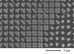
15. Producing small glass aspheric lenses in moderate to large quantities can be done by molding. A single mold with multiple forms can fabricate such optics in larger volumes with high optical quality. A group at the Centre of Micro/Nano Manufacturing Technology at Tianjin University (Tianjin, China) has created an off-spindle-axis (OSA) spiral grinding method that can be used to fabricate tungsten carbide molds to produce glass aspheric microlenses and microlens arrays. To grind a multiple aspheric lenslet array into the mold, off-spindle-axis spiral grinding is done using a four-axis ultraprecision machine with x, y, and z translational stages and a rotational axis. On-machine profile-error compensation analysis and subsequent compensation grinding steps maximize the form accuracy. (See “Off-spindle-axis spiral ground molds produce sub-micron-accurate aspheric microlens arrays,” May 2019 issue; http://bit.ly/2019TechRev15.)
16. Among the many advances in automotive lidar this year is the unveiling of a reflecting optical metasurface-based beam steerer by Lumotive (Bellevue, WA) as a part of its all-solid-state lidar system. In the device, a liquid-crystal coating on the metasurface allows tuning of its resonant subwavelength elements to steer the beam over a 120° angle with a random-access switching time of 25 μs and an aperture of up to 25 × 25 mm. The liquid-crystal metasurfaces (LCMs) are fabricated from silicon in a CMOS foundry using conventional materials and patterning processes. The Lumotive lidar system contains two LCMs, one each for transmit and one for receive, helping to reject extraneous light. (See “Metasurface beam steering enables solid-state, high-performance lidar,” July 2019 issue; http://bit.ly/2019TechRev16.)
Science and research
17. Truly random numbers, which are needed for cryptographic uses such as quantum-key distribution (QKD), are not as easy to generate as one might think. In fact, the “random” numbers generated by computers using even complex algorithms are only pseudorandom. Photonic systems that generate truly random numbers (say from laser fluctuations) have previously been bulky—now, scientists at Toshiba Research Europe (Cambridge, England) and the University of Leeds (Leeds, England) have created a small photonic integrated circuit-based quantum random number generator with two distributed-feedback lasers in the gain-switching regime—their on-chip interferometrically combined beams provide true random-number generation. (See “On-chip laser-based quantum device generates true random numbers,” July 2019 issue; http://bit.ly/2019TechRev17.)
18. After many false starts, an electrically pumped organic semiconductor diode has been created. Kyushu University (Fukuoka, Japan) researchers have created a laser structure containing films of the organic compound BSBCz both as the gain medium and as the distributed-feedback resonator, both deposited on glass—the device produced narrowline blue continuous-wave laser emission. The researchers have formed a startup called Koala Tech to produce the electrically pumped organic laser diodes, which they plan to integrate into OLEDs and organic electronic systems. (See “Electrically pumped organic diode laser comes to fruition,” July 2019 issue; http://bit.ly/2019TechRev18.)
19. When the Laser Interferometer Gravitational-Wave Observatory (LIGO) was upgraded to Advanced LIGO, improving its sensitivity fourfold, among the upgrades was a change from lithium niobate (LiNbO3) to rubidium titanyl phosphate (RbTiOPO4, or RTP) electro-optic modulators. (The length and alignment sensing schemes of the LIGO rely on optical sidebands generated by electro-optic modulators.) The new nonlinear optical material, fabricated by Raicol Crystals (Rosh Haayin, Israel), has allowed the Advanced LIGO to operate at high laser power levels (which were boosted from the original 10 W to 200 W) without experiencing thermal lensing or damage (see Fig. 5). (See “RTP optical crystal helps boost performance of LIGO,” September 2019 issue; http://bit.ly/2019TechRev19.)
20. Laser particle trapping, which has been used for the study of cells, particles, molecules, and atoms, can also aid in studying atomic nuclei. Researchers at Los Alamos National Laboratory (Los Alamos, NM) levitate a radioactive nuclear particle in a laser-based optical trap, wait for it to decay, and measure the magnitude and frequency of the particle's recoil (and associated kinetic energy). The recoil displacement is measured by position-sensitive photodiodes in real time, and the results are used to calculate the kinetic energy of the emitted alpha or beta particles or gamma photons. (See “Laser levitation and an optical trap enables nuclear recoil spectroscopy,” issue; http://bit.ly/2019TechRev20.)
About the Author

John Wallace
Senior Technical Editor (1998-2022)
John Wallace was with Laser Focus World for nearly 25 years, retiring in late June 2022. He obtained a bachelor's degree in mechanical engineering and physics at Rutgers University and a master's in optical engineering at the University of Rochester. Before becoming an editor, John worked as an engineer at RCA, Exxon, Eastman Kodak, and GCA Corporation.