After three decades of development, a new generation of lithography machines has now been shipped to large computer chip makers. It uses extreme ultraviolet (EUV) light at a wavelength of 13.5 nm to make silicon features down to a few nanometers in size on the memory chips and processors of tomorrow.
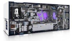
With more than 100,000 components, such an EUV lithography system is one of the most complex machines ever built. It is pumped by the most powerful laser system ever made in serial production. In total, it weighs 180 tons and consumes more than 1 MW electrical power. It costs $120 million and is sold out for years.
The big foundries have been waiting for it for quite some time. Now, major technical issues are solved thanks to a unique alliance between high-tech companies including Trumpf (Ditzingen, Germany), Zeiss (Oberkochen, Germany), and ASML (Veldhoven, Netherlands). It is worthwhile to take a look at the history of this technological masterpiece, and also to think about what might come next.
Why EUV?
Extreme ultraviolet (sometimes also called XUV) denotes soft x-rays with wavelengths between 124 and 10 nm or photon energies between 10 eV and 124 eV. The sun produces EUV; humans create it through synchrotrons, or from plasma.
Up until now, chip makers have used ultraviolet (laser) light to project complex patterns onto silicon wafers coated with photoresist. In a process analogous to the development of the old paper photos, these patterns are developed and become conducting or isolating structures within one layer. This process is repeated until the complex systems forming an integrated circuit such as a microprocessor are complete.
The development of such lithographic systems is driven by economy: Ever more computing power and storage capacity is needed while costs and power consumption must be lowered. This development can be described in a simple rule, well-known as Moore’s law, which says that the number of transistors in a dense integrated circuit doubles about every two years.
A major limitation comes from the laws of optics. German physicist Ernst Abbe found that the resolution of a microscope d is (roughly) limited to the wavelength λ of the light used in illumination:
where n is the refractive index of the medium between the lens and the object and α is the half-angle of the objective's cone of light. For lithography, substituting numerical aperture (NA) for n sin(α) and adding a factor k to the formula (because lithographic resolution can be strongly tweaked with illumination tricks), the minimum feasible structure, or critical dimension (CD), is:
This formula, which governs all lithographic imaging processes, makes obvious why the wavelength is such a crucial parameter. As a result, engineers have been looking for light sources with ever-shorter wavelengths to produce ever-smaller features. Beginning with UV mercury-vapor lamps, they moved to excimer lasers with a wavelength of 193 nm. The lithography industry received a surprise when Intel announced in May 2003 that it would drop the 157 nm excimer laser as a next step and instead go for EUV at a 13.5 nm wavelength. Problems with optical materials were seen as the major obstacle, and EUV seemed just a few development steps away.
It was reported at that time that Intel Fellow and director of the company's lithography capital equipment operations, Peter Silverman, presented a roadmap showing EUV to be deployed for the 32-nm node in 2009. That turned out to be by far too optimistic, and people had to find ways to exploit the 193 nm sources to achieve ever-smaller features through techniques such as immersion lithography and sophisticated illumination tricks.
An EUV light source for industry
Many problems have had to be solved for EUV lithography; first of all, a powerful light source was needed. In the early 2000s, discharge-plasma-based sources (such as touted by Xtreme Technologies) appeared most favorable, but before long laser-produced plasma sources showed that they were most viable for upscaling. Groups in Japan, Europe, and the USA worked hard on this approach.
Finally, the San Diego based company Cymer won the race with a system that uses a CO2 laser to create EUV radiation from a 30 µm droplet of tin. While they promoted a rather unstable 30 W source in 2007, it was 2014 when they first showed how to get to 250 W, a number that was regarded as the breakthrough for high-volume production. Driving up the efficiency of the EUV conversion process was a wonderful piece of applied research that made EUV lithography viable after all. To enable faster progress (and to secure its sole supplier), ASML purchased Cymer in 2012.
The eventual solution for making just enough EUV radiation for commercial viability is a machine that impresses even seasoned laser experts. It is based on the most powerful laser that was ever built in serial production: a 40 kW CO2 laser. The whole system needs a 1 MW power supply. As only the tiny fraction of 200 W of power is used for processing the wafer, cooling is a major issue.
The sole supplier of this technology is TRUMPF in Ditzingen, Germany. Trumpf owner and CTO Peter Leibinger is well aware of his company’s role: “If we fail, Moore's law will discontinue. Of course, the world doesn't depend on TRUMPF, but without TRUMPF, the chip industry couldn't do it,” he said in an interview in 2017.
Typical CO2 lasers from TRUMPF deliver some kilowatts of continuous-wave (CW) radiation. This is just right for cutting steel. For EUV, TRUMPF developed a laser that produces 40 kW of pulsed radiation at a repetition rate of 50 kHz. The laser, with its two seeders and four amplification stages, is so large that it has to be placed on a separate floor below the EUV machine.

To keep pace with the market demand, TRUMPF has invested heavily in an entirely new factory with 10 production bays just for these lasers. With 10 weeks to put them together, the company now has a capacity of 50 systems per year. At the time of writing, 44 systems were in the field with a total of 30 shipments expected in 2019.
Note—The resolution of the NXE:3400 systems is about 13 nm; this refers to formula (2) and the actual gate pitch. This is very different from the "nodes" often discussed the chip manufacturers. Originally, the nodes referred to the gate length of a transistor. Obviously, this can differ as a function of the process and, hence, of the manufacturer. Today, however, the node only refers to a certain process developed by a chip maker and does not correspond directly to the resolution of the optics. For example, chip makers tout 7 nm or 3 nm nodes referring to their proprietary processes using similar EUV machines.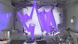
Cooperation is the key
While more than 1000 suppliers are involved overall, the core technology is made by Trumpf, Zeiss, and ASML. They developed rather unconventional forms of cooperation in the EUV project. Peter Leibinger from Trumpf called it a “virtually merged company” with an open-book policy and an extensive exchange of people and knowhow.
Zeiss SMT has a long history with ASML, as the company produced its first lithography optics for Philips in 1983; that business was spun off in 1984 and named ASML.
Together, Zeiss and ASML conquered the market for lithography systems well before EUV. In 2010, they already had about 75% market share for lithography systems. So far, they are the sole providers of industry-grade EUV systems. To foster the relation, ASML bought a 24.9% stake in Zeiss SMT for roughly one billion Euros in November 2016. Additionally, ASML promised to support Zeiss SMT’s R&D efforts for six years with 220 million Euros plus some investments support of 540 million Euros.
That money was much needed, as Zeiss was investing heavily in EUV. The company erected halls for manufacturing and metrology near Oberkochen, Germany; currently, it is completing preparation for the next generation of EUV optics with higher NA—another 700 million Euro investment. This includes high-vacuum chambers the size of a truck for metrology of the optical systems. The mirror surfaces that are tested in these chambers have a maximum tolerance of 0.5 nm, so they use the most precise alignment and metrology technology ever built in industry.
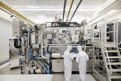
Final assembly of a 180 ton tool
Zeiss SMT has a giant high-tech facility, but it is topped in size by the manufacturing halls at the Veldhoven facilities of ASML. If you go there into the cafeteria, you may feel like you are on a campus in California. Many young people of all nations gather around and sip their lattes. This environment might reflect the fact that ASML has had to rapidly hire new staff to keep pace with their fast growth. In 2018 their staff grew 21%, now employing more than 800 PhDs and more than 7500 engineers in a total workforce of 23,000.
The buildings behind the cafeteria comprise the biggest cleanroom facility I have ever seen. In five by five halls, the EUV steppers machines are completed. The current top model, the NXE:3400B, weighs 180 tons and needs 20 trucks or three fully loaded Boeing 747s for shipment. The price tag is $120 million. It can process 125 wafers per hour with a resolution down to 13 nm.
In the second half of 2019, the shipment of an upgraded NXE:3400C was announced. It will feature higher-transmission optical elements, a modular vessel for significantly faster serviceability, and a faster reticle and wafer handler to support increased productivity. These devices achieve 170 wafers per hour throughput.
What comes after EUV?
The answer is—EUV. So far, EUV optics have reached an NA of 0.33. The next generation (ASML announced the machine as NXE Next) will have an NA of 0.55, enabling a resolution of less than 8 nm. It comprises larger optics, which explains the large and increased efforts at ZEISS SMT. Zeiss has already started production this year.
As a result of these combined efforts, it is clear that the technology is driven to its physical limits, enabling specifications that were hitherto not imaginable. For example, the wafers inside the lithography system are hold on special glass plates (so-called wafer clamps). They move at accelerations up to 3g, keeping the wafer in place with precision down to a nanometer. At the same time, the wafer is illuminated by EUV light at a heat load of 30 kW/m2 without losing its precise location.
Although a number of technical problems are still under discussion, the market seems very confident that EUV lithography will offer a substantial benefit for the semiconductor industry for the foreseeable future.
What comes after high-NA EUV? So far, there seems to be no serious answer yet. On the one hand, several research groups are preparing for shorter wavelengths. Two institutions of the German Fraunhofer Society completed a research project on “Beyond EUV” in 2016. They worked on reflective coatings (at IOF) and plasma sources (at ILT) for a 6.7 nm wavelength. A Swiss group summarized photoresist research in 2015. Alternative methods of nanopatterning such as stamping or e-beam lithography are evolving. A “patterning roadmap” in 2017 was an attempt to discuss their further development.
But if we look at this development from a distance, it seems that the complexity of lithographic technology has reached its viable maximum. What ASML and its allies currently build in their high-tech cathedrals showcases the largest and most advanced technological systems of our time. While this is stunning evidence of scientific and engineering mastery, it leaves the impression that further substantial progress will require a completely different approach to satisfy increased data storage and processing requirements.
About the Author

Andreas Thoss
Contributing Editor, Germany
Andreas Thoss is the Managing Director of THOSS Media (Berlin) and has many years of experience in photonics-related research, publishing, marketing, and public relations. He worked with John Wiley & Sons until 2010, when he founded THOSS Media. In 2012, he founded the scientific journal Advanced Optical Technologies. His university research focused on ultrashort and ultra-intense laser pulses, and he holds several patents.