Photonics for Datacenters: Integrated optics permeate datacenter networks
CYRIEL MINKENBERG, GREG FINN, and NICK KUCHAREWSKI
Datacenter networks are facing a key inflection point: while the reach of electrical interconnects keeps shrinking with increasing signaling rates, the capabilities of merchant switch silicon—defined as off-the-shelf, silicon-chip-based switches—are outpacing those of pluggable optical modules. This has created an optical bandwidth crunch that prevents optimal use of the most valuable assets—the servers.
Emerging technologies promise to address these issues by co-packaging fiber-optics links directly with the switch application-specific integrated circuit (ASIC). With production deployments planned in the near future, integrated optics will free datacenter networks from the cost, power, density, and architectural constraints limiting conventional optical interconnect solutions.
The state of datacenter networks
Over the past 10 years, the Ethernet ecosystem has come a long way. Networking gear was highly vertically integrated, based on proprietary hardware and software, leading to a poor price/performance ratio. The resulting lack of global network bandwidth imposed strong constraints on workload placement and was a poor match for data-intensive workloads. In effect, the network gated aggregate performance, posing a major obstacle to improving server utilization.
Many of the changes necessary to dismantle vertical integration in the networking ecosystem have materialized.1 This has been accomplished by far-reaching disaggregation (decoupling hardware from software) and commoditization, as exemplified by open-source-design networking boxes built around merchant switch silicon, open-source networking software stacks, and the advent of software-defined networking (SDN) and programmable forwarding and data planes.
Despite these improvements, the fundamental problem of global performance being gated by scarce networking resources still exists. Disaggregation has uncovered a new bottleneck—that is, the burden of cost has shifted from the switch and router boxes to the optical links that are needed to interconnect them in a warehouse-scale datacenter.
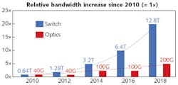
Merchant silicon switch ASICs have been on an exponential growth curve. Since 2010, single-chip capacity has doubled every two years through a combination of increasing channel count and rate. Optical modules, on the contrary, have been on a much more gradual incline, creating a gaping chasm in their respective levels of integration (see Fig. 1).
Currently, a single-switch ASIC provides as many as 256 channels at 50 Gbit/s each.2 Optical modules, by contrast, are severely under-integrated, currently providing a maximum of four channels. This discrepancy is also reflected in the relative cost per capacity, which has dropped much faster for switch capacity, to the point where in some cases the cost of the optics to populate the interfaces of a 1RU (1 rack-unit) switch exceeds the cost of the unit itself.
This lack of integration can be attributed to several factors. First, optical modules are complex micro-optical systems, comprising an array of discrete components from often widely differing technologies, typically hand-assembled into optical circuits. And although silicon photonics has brought about improvements in transceiver manufacturing, the deployment model based on discrete pluggable modules has not changed, precluding more substantial integration benefits.
Another compounding factor is a splintering of the market and the associated plethora of optical interfaces defined by both standards and multi-source agreements (MSAs), with its negative consequences for economies of scale of each individual interface.
In addition to cost, faceplate density and power consumption have also become constrained by pluggable transceiver optics. Density is limited by the number of modules (of a given form factor) that can fit on a 1RU faceplate. This arrangement concentrates a lot of power dissipation in a small area and obstructs the airflow needed for cooling. A substantial amount of energy is consumed for electrical signaling from switch ASIC to faceplate-mounted modules across a PCB. As per-channel signaling rates keep increasing, this requires more pre- and post-conditioning to maintain signal integrity.
Enter integrated optics
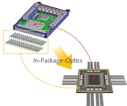
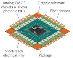
To ease the pluggable module bottleneck, a high degree of integration can be achieved by co-packaging optical engines along with the main ASIC on a common substrate (see Fig. 2). This reduces input/output (I/O) power by limiting electrical signaling to intra-package distances, reduces cost by increasing channel count per optical sub-assembly and by eliminating discrete transceiver packaging as well as high-speed PCB traces, and enables high-density optical faceplate connectors.The practical realization of such an optoASIC requires 1) high-density, low-cost photonic integrated circuits (PICs) along with energy-efficient driver/receiver circuits to implement the optical engines, 2) packaging technology to accommodate a substantial number of such engines in a single package with a high-capacity switch ASIC, and 3) low-power electrical interfaces to connect engines and ASIC.
Although there is little doubt about the appeal and technical feasibility of integrated optics, we also need to consider how this technology fits market needs, and how it slots into the existing supply chain and business model of datacenter networking gear.3-7
Silicon photonics platforms
Silicon photonics allows the integration of many different optical devices onto a single silicon die.7 However, there are a variety of silicon photonics platforms and integration approaches. These are not all created equal when it comes to suitability for integrated optics solutions.
Ease of manufacturing should drive the choice of the optimal silicon photonics platform. A key observation is that getting light into and out of the silicon is the main driver of manufacturing cost and complexity. This leads to a conclusion that runs counter to the intuition learned from decades of scaling down device features in CMOS devices. In photonics, scaling waveguide geometries down to the deep sub-micron range turns out to be counterproductive to the core objective of achieving high-throughput, high-yield manufacturing.
A multi-micron-waveguide platform has several crucial advantages over submicron platforms. A large-waveguide platform is much more tolerant to process variations, leading to higher yield. Large waveguides enable passive-alignment structures for low-loss, high-throughput fiber attachment. They also exhibit lower optical loss and polarization-independent performance, can be designed to be single-mode, and can handle higher optical power. These characteristics also enable wavelength-division multiplexing (WDM), which greatly improves bandwidth density.
Another core advantage is the ability to integrate devices from other materials systems—for instance, III-V-based light sources—by means of low-loss, high-throughput passive alignment.
Next, despite the large geometry, tight waveguide bends can be manufactured, enabling compact structures to match the density (pitch) of both ASIC SerDes (serializers/deserializers that convert data between serial and parallel interfaces in each direction) and fiber arrays.
Another crucial component is the modulator. A larger mode size enables the use of smaller and more energy-efficient electro-absorption modulators (EAMs), as opposed to the Mach-Zehnder-type modulators needed in submicron platforms. This increases bandwidth density and lowers power consumption. Moreover, these modulators can be driven by single-stage, low-voltage CMOS drive circuits, further increasing the energy-efficiency advantage, and have been shown to be amenable to operation beyond 100 Gbit/s.
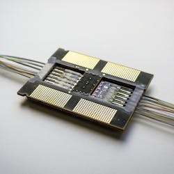
Rockley Photonics has developed a technology platform for In-Package-Optics solutions exhibiting all of these characteristics and has implemented a prototype optoASIC that demonstrates technical feasibility and power-saving potential (see Fig. 3).8Implications for datacenter network architecture
Integrated optics will drive down the cost of optical links by giving rise to higher-channel-count optical engines, lower total component cost (fewer parts, less packaging), fewer assembly steps, and high compound yield. Integration also reduces energy consumption by minimizing the energy spent on electrical I/O. In addition, the elimination of faceplate-mounted modules improves airflow and increases the number of fibers that can be accommodated through dense optical connectors.
Perhaps even more important than improving cost, power, and density metrics are the potential implications for datacenter network architecture as a whole. This technology marks a fundamental shift in the economics of reach—the very same economics that underpinned the architectural decisions that have led to today’s network architectures.9 As soon as bandwidth-distance becomes much less of a constraining factor than it traditionally has been, architects will be free to design towards more productive optimization criteria.
Datacenter networks will finally be liberated from the bandwidth-delay-product constraints that have so long dictated architectural decisions. With these limitations out of the way, the full potential of a datacenter’s computing power can be unlocked. The imminent era of integrated optics will provide a sea of possibilities for repartitioning existing designs and inventing completely new ones, from the chip and box level all the way up to the entire datacenter.10 The optoASIC revolution has only just begun.
ACKNOWLEDGEMENT
In-Package-Optics is a trademark of Rockley Photonics Limited.
REFERENCES
1. J. Hamilton, “Data center networks are in my way,” Stanford Clean Slate CTO Summit, Stanford, CA (2009).
2. T. Prickett Morgan, “Feeding the insatiable bandwidth beast,” nextplatform.com (Apr. 30, 2018).
3. B. Arimilli et al., “The PERCS high-performance interconnect,” IEEE Hot Interconnects 18, Mountain View, CA, 75–83 (Aug. 2010).
4. K. Hasharoni et al., “A high end routing platform for core and edge applications based on chip to chip optical interconnect,” Proc. OFC, paper OTu3H.2, Anaheim, CA (2013).
5. A. V. Krishnamoorthy et al., J. Lightwave Technol., 35, 15, 3103–3115 (Aug. 2017).
6. M. Akhter et al., “WaveLight: A monolithic low latency silicon-photonics communication platform for the next-generation disaggregated cloud data centers,” IEEE Hot Interconnects 25, Santa Clara, CA, 25–28 (Aug. 2017).
7. C. Minkenberg et al., J. Opt. Commun. Netw., 10, 7 (Jul. 2018).
8. G. Reed and A. Knights, Silicon Photonics: An Introduction, Wiley (Mar. 2004).
9. C. Minkenberg et al., “Redefining the economics of reach with integrated optics,” IEEE HPSR ‘18, Bucharest, Romania (Jun. 2018).
10. N. Kucharewski et al., “Network architecture in the era of integrated optics,” Proc. OFC, paper M3J.7, San Diego, CA (2018).
Cyriel Minkenberg is a system architect, Greg Finn is vice president of business development, and Nick Kucharewski is chief commercial officer located in the San Jose, CA office, all at Rockley Photonics, Oxford, England; e-mail: [email protected]; www.rockleyphotonics.com.


