Market Insights: How advanced packaging can help align the evolution of photonic ICs with Moore's Law
![FIGURE 1. Moore's Law representation of the electronic (red) and photonics (blue) number of elements vs. year. Electronics doubles every 1.99 years with a high correlation coefficient of 0.95; in contrast, photonics doubles only every 3.42 years, and with a much lower correlation coefficient of 0.72 [1-3].](https://img.laserfocusworld.com/files/base/ebm/lfw/image/2017/03/content_dam_lfw_print_articles_2017_03_1703lfw_mi_f1.png?auto=format%2Ccompress?w=250&width=250)
LARRY TAROF
Few would disagree with the observation that the information age has ridden the tailwind of Moore's Law, which famously and accurately predicted that the number of transistor elements on integrated chips (ICs) would double every two years. However, Moore's Law is fast approaching a physical boundary as transistor size approaches atomic limits and rising interconnect resistance dominates power consumption. As a consequence, the industry is turning to photonic ICs (PICs), which it widely views as the "next big thing" necessary to create tomorrow's datacenters.
Despite being unencumbered with the challenging technology limits of minute transistor size, the number of elements on a PIC doubles only every 3.42 years, and with more scattered correlation coefficient (see Fig. 1). It's clear that PICs are not delivering on the hope and promise at the rate the industry had hoped for. A significant source of these delays can be traced to the development ecosystems for application-specific ICs (ASICs) in general, and to PICs in particular.
Unique challenges for PICs
The flow of principal interactions in a conventional electronic ASIC ecosystem encompasses an ongoing iteration loop consisting of ASIC design (the "brains" of the operation), the foundry, and test/characterization (see Fig. 2a). This loop ensures the ASIC does what is intended.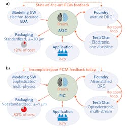
The foundry, with its mature design rule checker (DRC), interacts with the modeling software, which also includes the electronic design automation (EDA) necessary to facilitate rapid logic placement as an ASIC design progresses. This process ensures that intricate device performance calculations are consistent with what the foundry process actually does. The ASIC design is adjudicated on a per-application basis.
In this ecosystem, packaging is a satellite operation that consumes only 12% of the cost, consistent with a large, approximately 30 μm target. This well-oiled ecosystem has been ideal to sustain the curve of Moore's Law to date.
Because of the success of this ecosystem in conventional ASICs, PICs have sought to apply an analogous approach. However, this poses significant impediments to the further progress of PICs. First, the model for photonic DRC is still evolving. Foundries tend to have differing design rules, and PICs often require exceptions to optimize their performance. This is a by-product of the varying epitaxial and processing requirements for different optoelectronic devices that each research group, as foundry precursors, has previously solved in its own way.
Second, while the software modeling for PICs is extremely sophisticated and employs multi-disciplinary physics, it is still cumbersome to use and requires a comparatively higher skill set. This is understandable because photonics remains more complex, even though electronics are today successfully addressing difficult 2D and 3D short transistor effects.
The evolution of ASICs had hit a similar brick wall until electronic design automation came online at about the 10,000 transistor mark early in the Moore's Law journey. PICs are integrating the same number of elements today, but with more complex and varied optoelectronic devices than what traditional transistors confronted. Thus, the industry urgently needs electronic design automation to evolve more quickly.
Third, and perhaps most important, packaging dominates PIC costs today, which is not surprising. Optical alignment requirements alone (typically about 1 μm) are extremely stringent, and there are also difficult thermal issues to address, such as resolving the mechanical stress arising from the disparate coefficients of thermal expansion (CTE) of materials used. Another challenge unique to PIC packages is the management of operational and assembly thermal profiles characteristic of heat-sensitive optoelectronic components.
In short, there is poor alignment between the cost and the end goals for a PIC ecosystem that attempts to mimic an ASIC system (see Fig. 2b). The impact of this is evident in the Moore's Law curve for photonics.
Potential solutions via PIC packaging
If we recognize that packaging is the dominant cost, however, then the ecosystem can be adjusted to address some of these impediments (see Fig. 3). Some items that work well for ASICs remain.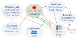
Among them is the iteration loop between the PICs ("brains"), the foundry, and test/characterization. This is not a dominant contributor to cost because photonics foundries can avoid the expensive capital investment needed for nanoscale ASICs.
In addition, PIC design and foundries still need to manage the DRC issue. But as PICs become more economically important, we can expect the industry will address this quickly, together with photonics EDA. But there are still important differences here.
First, a prominent new iteration loop emerges between PIC design, packaging, and test/characterization. Second, materials for packaging become front and center. For example, CTE, signal loss [as represented by tan(delta)], and adhesive properties that affect both the optical signal and the thermal/stress profile will all become more critical design considerations for the in-feed for PIC packaging as well as the modeling software. Third, as modeling software grows ever more sophisticated and user-friendly, it will not only apply to the PICs, but to the packaging as well. Fourth, and equally important, PIC applications are bundled in a fundamentally different manner than ASIC applications because whereas board and module design are usually rote for electronics, they pose a complex undertaking for photonics.
The physical entity that is adjudicated for a given application is not the PIC alone, but rather a packaged module. Therefore, PIC design must advance with packaging as a unified entity.
From a business, economic, and structural point of view, this necessitates the emergence of more joint development models than have been observed in the past. But if we align as an industry in this direction, we stand a fighting chance of resolving some of the key impediments to PIC development. This, in turn, may help the industry to find a turning point in which Moore's Law can apply more closely to PICs as it has to ASICs for nearly half a century. This will help fuel the applications that tomorrow's datacenters require to drive the 5G, Internet-of-Things, zettabyte economy.
REFERENCES
1. See https://goo.gl/lr2pW0.
2. See https://goo.gl/HcaFbF.
3. M. Smit et al., Laser Photon. Rev., 6, 1, 1-13 (2012).
Larry Tarof, Ph.D., is Chief Photonics Scientist at Jabil Circuit, St. Petersburg, FL; e-mail: [email protected]; www.jabil.com.