PHOTONICS APPLIED: COMMUNICATIONS: Optical technologies scale the datacenter

HONG LIU and RYOHEI URATA
An increasing fraction of computing and data storage is migrating to a planetary cloud of warehouse-scale datacenters.1 While substantial traffic will continue to flow between users and these datacenters across the Internet, the vast majority of overall data communication is taking place within the datacenter.2 For example, a datacenter with 100,000+ servers, each capable of 10 Gbit/s (or 10G) of bandwidth, would require an internal network with 1 petabit per second of aggregate bandwidth to support full-bandwidth communication among all servers. Leveraging existing datacenter topologies, switching, and interconnect technologies makes it difficult and costly to realize such scale and performance.
Optics plays a critical role in delivering the potential of datacenter networks and addressing the challenges. However, fully realizing this potential requires a rethinking of the optical technology components traditionally used for telecom environments; optimizations must specifically target deployment within a datacenter environment.
Evolution of datacenter network architecture
Over the past decade, advances in merchant silicon switching (electrical/CMOS-based packet switches) and software defined networking (SDN)—whereby the control plane is implemented with servers, separated from the switching equipment—have evolved datacenter networks from traditional hierarchical networks with oversubscription (bandwidth provisioned is less than maximum possible peak/demand bandwidth) to a nonblocking fabric with little or no oversubscription at each layer.3
Modern datacenter architectures use an array of small pods (or networking clusters) composed of identical switches built with merchant switch silicon, to create the large-scale networking fabric with any-node-to-any-node connection (see Fig. 1). The access layer could be a traditional top-of-rack (ToR) switch performing layer 2 (L2 or Data Link Layer) switch function to move packets around the network. There is full bisectional bandwidth (no oversubscription) with extensive path diversity within the pod and among the pods.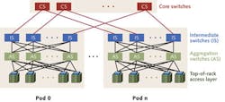
Large-server-count, scale-out datacenters pose many technical and deployment challenges at and beyond the petabyte scale. Besides software complexity, there are many limitations with existing technologies, including: 1) Management: The number of electrical packet switches (EPSs) substantially complicates management and overall operating expenses; 2) Cost: The cost of optical fiber cables and optical transceivers would dominate the overall cost of the network fabric; 3) Power: The power of optical transceivers would limit the port density as bandwidth scales; and 4) Cabling complexity: Millions of meters of fiber would be required to interconnect large-scale datacenters, presenting an extremely daunting deployment and high operational overhead.
Enabling optical technologies
Optics has already played a critical role, mostly as interconnect media, in delivering on the potential of the datacenter network. Various emerging optical technologies are candidates to address the technical and operational challenges of scale-out networking and improve the performance and efficiency of large datacenters.
The use of wavelength-division multiplexing (WDM) transceivers as a first-class entity for modular datacenters is one enabler for future datacenter networks (see Fig. 2).4,5 For connections to and from the pods to core switches, traditional parallel optical transceivers are replaced with integrated WDM transceivers (40G, 100G, 400G, and beyond) to aggregate signals from multiple channels with a common destination over a single strand of fiber.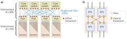
Within the fabric of these pods and core switches, interconnect technologies will similarly be at higher speeds (≥40G) while needing to maintain fixed cost, size, and power per bandwidth. In this application area, integrated parallel optical transceivers could provide a very efficient way to scale the bandwidth.
To meet the server and network bandwidth growth, new optical technologies at the device level, more complex modulation techniques or lane aggregation, and photonic packaging are all required to scale data rate, power, cost, and space/density. Within this optimization, the choice of singlemode or multimode fiber needs to be carefully considered along with corresponding compatible technologies.
High-speed VCSELs, DFBs, and silicon photonics
Low-power, inexpensive vertical-cavity surface-emitting lasers (VCSELs) and multimode fiber (MMF) already play a critical role for communication at 10 Gbit/s within the datacenter. Although significant progress has been made in higher-speed VCSELs using alternate materials, overcoming the reliability and yield hurdles to scale VCSELs significantly beyond 20 Gbit/s link speeds has thus far proven difficult.6 Furthermore, traditional VCSELs coupled with MMF have a limited reach-bandwidth product due to modal dispersion. At 10 Gbit/s, the associated reach is already insufficient to cross a single datacenter building and this maximum reach shrinks rapidly with higher data rates.
Higher-power, more expensive distributed-feedback (DFB) lasers and singlemode fiber (SMF) are often used in the datacenter to cover the reach beyond 300 m at 10 Gbit/s. As we scale from 10G to 25G per lane, DFB lasers can use more novel quaternary materials such as indium gallium aluminum arsenide/indium phosphide (InGaAlAs/InP) that exhibit better high-temperature performance and higher speeds. Novel DFB laser structures such as short-cavity and lens-integrated surface-emitting DFB lasers have also been demonstrated (see Fig. 3).7,8 These approaches provide higher device bandwidth and a narrower spectrum in comparison to their VCSEL-based counterparts to increase interconnect bandwidth and reach while maintaining low power consumption and cost.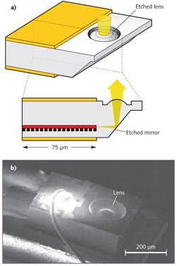
In the past decade, significant advances have been made in silicon photonics to address the energy efficiency and cost of traditional optical transceivers using III-V compound materials. Silicon (Si), although not the material of choice for semiconductor lasers due to its indirect bandgap, has good thermal conductivity, transparency at the traditional telecom wavelengths, low noise for avalanche multiplication (from high electron/hole impact ionization ratio), and, most importantly, can leverage existing Si CMOS fabrication processes developed for the electronics industry.
Silicon photodetectors are the oldest and perhaps best understood silicon photonics devices. For wavelengths below 1000 nm, Si is a low-cost and highly efficient photodetector. Low-loss waveguides in Si for wavelengths above 1000 nm have also been demonstrated, allowing the creation of higher-functionality waveguide-based devices as well as chip-level interconnection of various components to realize devices such as photonic integrated circuits (PICs).
Other recent advances in the main building blocks of silicon photonics include high-efficiency germanium (Ge) photodetectors, high-speed Si modulators with extremely small switching energy, and Ge/Si lasers.9-11 The intimate integration of electronics with photonics allows the realization of higher bandwidth at lower power, giving silicon photonics the potential to improve datacenter flexibility, energy efficiency, and cost, contingent on overcoming various packaging and integration hurdles.
WDM
Space-division multiplexing (SDM; where information is being transferred across multiple physically separated links) and WDM both take advantage of the natural parallelism of data lanes in computer architectures and electrical/CMOS switches, and are two widely used multiplexing techniques in the datacenter. However, the corresponding use of MMF/SDM-based technologies of VCSEL arrays, ribbon fibers, and multifiber termination push-on (MTP) and multifiber push-on (MPO) connectors can incur a significant portion of the entire datacenter network cost and cable volume.
There is a large savings with SMF-based technologies in cable cost and volume through multiple generations of networking fabric when the interconnect bandwidth scales from 10GE (Gigabit Ethernet) to 40GE/100GE to 400GE (see table). It should be noted that there is potentially both a capital expenditure (capex) and operational expenditure (opex) advantage with SMF. The fiber is installed once for a particular interconnect speed. Subsequent increases in speed only require adding wavelength channels, with the fiber infrastructure remaining in place.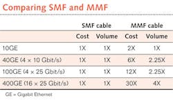
Wavelength-division multiplexing is widely used in metro and long-haul transmission and has allowed the telecom industry to gracefully scale bandwidth over the past several decades. It is clear that WDM will need to make its way from these traditional telecom application areas to the short-reach datacenter interconnect area to reduce the optical cabling and interconnection overhead costs and scale to ever-increasing link bandwidths. In other words, spectrally efficient optics, where a large number of wavelength channels are packed onto a single strand of fiber, will need to be used in next-generation datacenter transceivers.
But meeting datacenter economies and scale requires WDM performance without an associated explosion in power and cost. In traditional telecom applications, the approach was to spend more at the link end points to maximize the spectral efficiency of long-distance fiber links, as evidenced by the activity in research and development on coherent transmission devices and systems over the past several years. Within the datacenter, fiber resources are much more abundant, cheap, and easy to deploy. Thus, the transceiver cost must be aggressively reduced so as not to dominate the cost of the datacenter interconnect fabric.
Transceivers with high power consumption present thermal challenges and limit EPS chassis density. In the datacenter, non-retimed (limited electrical signal regeneration), uncooled transceiver solutions are thus preferred. Photonic integrated circuits, low-threshold lasers with better temperature stability, and silicon photonic modulators with low switching energy hold promise for further reducing power.
Optical interconnects for the datacenter typically span between 10 m and 2 km across multiple buildings within the same campus. Datacenter transceivers must account for the optical loss from fiber cables and patch panels, and the photonics highway must align seamlessly with the electrical switch fabric in bandwidth and speed. Today, multiple standards-based interconnect technologies provide cost-effective and power-efficient WDM transceiver solutions. Moving forward, further integration in the transceiver to align with the bandwidth and speed from merchant switch silicon will be necessary.
Finally, there will continue to be a tradeoff between spectral efficiency, power consumption, fanout to different paths, and cabling complexity of the datacenter interconnect and network. For the intra-building network, building a large switch fabric with rich connectivity is desirable; hence, spectral efficiency tends to be traded for lower-power, cheaper transceiver cost and a network fabric with abundant path diversity.
REFERENCES
1. L. Barroso and U. Hölzle, The Datacenter as a Computer, Morgan & Claypool Publishers (May 2009).
2. C. Lam et al., "Fiber optic communication technologies: What's needed for datacenter network operations," IEEE Commun., 48, 7, 32–39 (July 2010).
3. OpenFlow web site; www.openflow.org.
4. H. Liu et al., "Scaling Optical Interconnects in Datacenter Networks," Proc. 2010 18th IEEE Hot Interconnects (HOTI) Symp., 113–116.
5. M. Al-Fares et al., "A Scalable, Commodity, Datacenter Network Architecture," 2010 ACM SIGCOMM conference, New Delhi, India.
6. T. Anan et al., "High-speed 1.1-μm-range InGaAs VCSELs," 2008 OFC/NFOEC, conference paper OThS5, San Diego, CA.
7. T. Fukamachi et al., "95°C uncooled and high power 25-Gbps direct modulation of InGaAlAs ridge waveguide DFB laser," 2009 ECOC, Vienna, Austria.
8. K. Shinoda et al., "Monolithic lens integration to 25-Gb/s 1.3-μm surface-emitting DFB laser for short-reach data links", 2010 15th OECC, Sapporo, Japan.
9. L. Vivien et al., "42 GHz p.i.n Germanium photodetector integrated in a silicon-on-insulator waveguide," Opt. Exp., 17, 8, 6252–6257 (2009).
10. A. Liu et al., "Recent development in a high-speed silicon optical modulator based on reverse-biased pn diode in a silicon waveguide," Semicon. Sci. and Technol., 23, 6, 064001 (2008).
11. J. Liu et al., "Ge-on-Si laser operating at room temperature," Opt. Lett., 35, 5, 679–681 (2010).
Hong Liu is a principal engineer and Ryohei Urata is a member of the technical staff in the Advanced Platform Technology group at Google, 1600 Amphitheatre Parkway, Mountain View, CA 94043; e-mail: [email protected]; www.google.com.