Terahertz spectroscopy and imaging of 3D semiconductors breaks the nanometer barrier
Researchers at Applied Research & Photonics (ARP; Harrisburg, PA) have broken the nanometer barrier for analysis of semiconductor layers in a 3D volume.1 The following is an excerpt with modifications from the paper describing the work performed:
For many integrated circuit and high speed transistor applications the strain in the epitaxial layers of a semiconductor is relieved by introducing misfit dislocations that has inherent strain in their lattice structure. Therefore, controlling the growth conditions and a strategic design of the structure is necessary for minimizing the density of dislocations threading through device layers grown on top of the relaxed buffer layer. While visualization of these structures on a nanometer scale is important, the time-domain spectroscopic investigation yields additional information about the molecular nature of these structures that are also important.
RELATED ARTICLE: Terahertz reflectometry nondestructively inspects foil seals
Especially, terahertz spectroscopic inspection on a layer-by-layer basis plays a key role for the success in creating controlled 3D semiconductor structures. The need to prevent strain relaxation in thin layers or to control the density and distribution of defects in relaxed structures has led to extensive research on strain relaxation mechanisms and also on the properties of the defects which are required to relieve the strain. Therefore, in addition to the spectroscopic analysis, 3D visualization of these structures on a nanometer scale is of paramount importance.
In particular, the capability of sub-surface inspection on a layer-by- layer basis in a non-destructive and non-contact mode is the key for success in creating such 3D structures.
In what follows, ARP describes terahertz time-domain spectroscopy and high resolution reconstructive imaging via terahertz reflectometry for strain relaxed SiGe/Ge/Si structures. Two cases are investigated. Grown Ge layer on Si <001> substrate is inspected by terahertz pump-probe signals as a function of thickness yielding layer-by-layer spectroscopic information of the epitaxial structures. Then, another sample is inspected where SiGe layer was grown on top of the Ge buffer of the first case, also via layer-by-layer terahertz pump-probe technique. The spectra are analyzed for their identifying features of the epitaxially grown semiconductor layers.
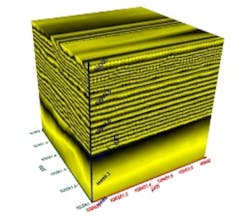
In addition, both samples were inspected by 3D sub-surface imaging. A side by side comparison is attempted. Clear visualization of the lattice stacking fault and defects was demonstrated that could shed light for streamlining the process parameters. We utilized terahertz non-contact multispectral reconstructive imaging to investigate aforementioned grown semiconductor layers.
An algorithm of gridding with inverse distance to power equations has been used for reconstructive imaging. The images are further analyzed via graphical means to measure the interface features and layer thicknesses. Nanoparticles with sub-nanometer dimensions were found within the semiconductor layers, breaking the nanometer boundary for this imaging analysis.
REFERENCE:
1. A. and AK Rahman, Journal of Biosensors and Bioelectronics 7, 4, 1000229 (2016); DOI: 10.4172/2155-6210.1000229.
SOURCE: Applied Research & Photonics; http://npic.us
About the Author

Gail Overton
Senior Editor (2004-2020)
Gail has more than 30 years of engineering, marketing, product management, and editorial experience in the photonics and optical communications industry. Before joining the staff at Laser Focus World in 2004, she held many product management and product marketing roles in the fiber-optics industry, most notably at Hughes (El Segundo, CA), GTE Labs (Waltham, MA), Corning (Corning, NY), Photon Kinetics (Beaverton, OR), and Newport Corporation (Irvine, CA). During her marketing career, Gail published articles in WDM Solutions and Sensors magazine and traveled internationally to conduct product and sales training. Gail received her BS degree in physics, with an emphasis in optics, from San Diego State University in San Diego, CA in May 1986.