RAMAN SPECTROSCOPY: Plastic SERS sensor is mass-producible, disposable
In surface-enhanced Raman spectroscopy (SERS), a sensing surface is modified by roughening or the addition of nanoscale features; the modification boosts Raman scattering from molecules on the surface by many orders of magnitude. This highly sensitive form of spectroscopy has been commercialized and widely used to sense minute amounts of organic substances such as foods, drugs, bacteria, pesticides, indicators of cancer, and many others.
In 2006, Mesophotonics (Southampton, England), a spinoff of the University of Southampton, introduced the first all-in-one SERS toolkit, which included a spectrometer, SERS substrates, and software; the nanostructured, silicon-based “Klarite” substrates provided highly reproducible SERS signals, leading to the wide use of SERS in the real world. (Mesophotonics is now a part of Renishaw Diagnostics; Klarite sensors are used in pharmaceuticals and biosensing.)
Now, Martin Charlton, who founded Mesophotonics, and his team at the University of Southampton have developed a version of the Klarite substrate that is not only more sensitive, but is also disposable.1 They achieved this by using plastic instead of silicon as the sensor base, using roll-to-roll (R2R) and sheet-level nanoimprint fabrication techniques to replicate SERS sensors in potentially large quantities.
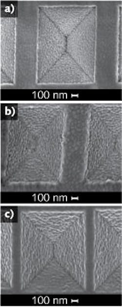
The original Klarite surface contains gold-coated inverted pyramidal pits with a 2000 nm pitch length and a 1500 nm pit diameter. An improved version with a 1250 nm pitch and a 1000 nm pit diameter shows an 800% average sensitivity improvement; this is the version that has been successfully transferred to a plastic base.
Two ways to fabricate
In the sheet-level version of the new process, a “positive” master template is fabricated from silicon by electron-beam patterning, etching, and coating with an anti-stick film (see figure). The master template is used to form interim “negative” templates from a soft PMMA polymer, which are then UV-cured. These interim templates are then used in a similar replication process to form the final “positive” textured surfaces.
In the R2R version of the process, a nickel shim is electroplated on the silicon master, detached, and welded to an embossing reel. A PMMA carrier web coated with a UV-curable lacquer is embossed by the reel and simultaneously UV-cured through the transparent film, then quickly post-cured and laminated with a protective foil. In both cases, the nanostructure is coated with a gold film.
The two methods show slight differences in the grain structure of the gold layers; the researchers expect that the result will be slightly different levels of Raman amplification—results that will be discussed in a future paper. Reproducibility of Raman measurements for the R2R and sheet-level fabrication processes are 5% and 9.41%, respectively.
“This development (transfer of the substrate from silicon to plastic) takes a big step forward in bringing the cost of manufacture down,” says Charlton. “Another advantage is that we can increase the active area size considerably with little impact on production cost, which makes them more flexible for customer applications.”
Charlton notes that the development of the disposable SERS substrate was undertaken via the FP7 PHOTOSENS project, which involves a number of other European Union partners. “We have drawn on the expertise of these partners to get this to work,” he says. “In particular, Nanocomp (Lehmo, Finland), 3D AG (Baar, Switzerland), and VTT (Espoo, Finland) have solved considerable technical issues to make the pattern transfer to plastic work. We hope to commercialize the new plastic version of the sensors though our Renishaw and other project partners (Philips).”
Upcoming research
The researchers plan to work on the specialized surface chemistry that enables the SERS sensors to be made specific to a particular molecule. “The longer-term plan is to integrate further functionality into the SERS sensor by incorporating underlying waveguide structures in the plastic to better couple the incoming pump light, and to provide dual sensing methodologies,” says Charlton. “For example, we could combine SERS with photonic-crystal sensors to provide better quantification of signal data (SERS is notoriously unsuitable to give highly quantitative measurements, but very good at giving present/not-present detection at very high sensitivities). Combining the two different sensor technologies into one system would enable new applications, he notes.
“We believe that overall there is great potential for a new field of plastic-based integrated optical components that go far beyond the current demonstrator,” he says. “We are working on many such devices, including plastic-based lasers, light sources, sensors, and optical interconnects.”
REFERENCE
1. S. Z. Oo et al., Opt. Exp., 21, 15 (July 29, 2013).
About the Author
John Wallace
Senior Technical Editor (1998-2022)
John Wallace was with Laser Focus World for nearly 25 years, retiring in late June 2022. He obtained a bachelor's degree in mechanical engineering and physics at Rutgers University and a master's in optical engineering at the University of Rochester. Before becoming an editor, John worked as an engineer at RCA, Exxon, Eastman Kodak, and GCA Corporation.

