Organic semiconductor electrical conductivity doubles with Stanford fabrication method
Stanford, CA--Researchers at Stanford University led by chemical engineer Zhenan Bao have improved the ability of electrons to move through organic semiconductors, increasing their potential to be used as foldable smartphones, in better high-definition television screens, and in solar clothing that turns sunlight into electricity for recharging your iPad. The feat was accomplished by packing the molecules closer together as the semiconductor crystals form in a technique known as "straining the lattice." Bao and her colleagues have more than doubled the record for electrical conductivity of an organic semiconductor and shown an eleven-fold improvement over unstrained lattices of the same semiconductor. The research will be published in the journal Nature.
"Strained lattices are no secret. We've known about their favorable electrical properties for decades and they are in use in today's silicon computer chips, but no one has been successful in creating a stable strained lattice organic semiconductor with a very short distance between molecules, until now," said Bao.
Bao's team used a solution-shearing technique similar to a coating process well known in the semiconductor industry. Solution shearing involves a thin liquid layer of the semiconductor sandwiched between two metal plates. The lower plate is heated and the upper plate floats atop the liquid, gliding across it like a barge. As the top plate moves, the trailing edge exposes the liquid to a vaporized solvent. Crystals form into a thin film on the heated plate. The engineers can then "tune" the speed at which the top plate moves, as well as altering the thickness of the solution layer, the temperature of the lower plate and other engineering factors, to achieve optimal results.
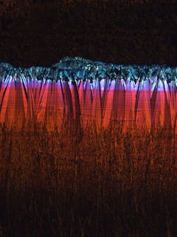
The crystals form in differing structures based on the speed at which the top plate moves. The engineers tested the various crystalline patterns for their electrical properties. They found that optimal electrical conductivity was achieved when the top plate moved at 2.8 mm/s, a speed in the middle of the range they tested. "In comparing the photographs of the crystals, it is not the longest, straightest structures that result in the best electrical characteristics," said Bao, "but the one with a shorter, yet highly consistent pattern."
In the paper, Bao describes her new technique as general enough as to be applicable to other materials that might someday yield even better electrical characteristics in a wide range of organic semiconductors.
SOURCE: Stanford University; http://news.stanford.edu/pr/2012/pr-bao-organic-semiconductors-122111.html
About the Author

Gail Overton
Senior Editor (2004-2020)
Gail has more than 30 years of engineering, marketing, product management, and editorial experience in the photonics and optical communications industry. Before joining the staff at Laser Focus World in 2004, she held many product management and product marketing roles in the fiber-optics industry, most notably at Hughes (El Segundo, CA), GTE Labs (Waltham, MA), Corning (Corning, NY), Photon Kinetics (Beaverton, OR), and Newport Corporation (Irvine, CA). During her marketing career, Gail published articles in WDM Solutions and Sensors magazine and traveled internationally to conduct product and sales training. Gail received her BS degree in physics, with an emphasis in optics, from San Diego State University in San Diego, CA in May 1986.