IR DETECTORS: Low-cost organic photodiodes reach into the infrared
IAN H. CAMPBELL
Organic photodiodes are of interest for many applications due to their simple low-temperature processing; high quantum efficiency; compatibility with large-area, flexible, and curved substrates; and low cost. To date, organic photodiode research is focused on solar energy applications. Despite this, most organic photodiodes and solar cells are sensitive only in the visible spectrum.1
For solar energy, communication, and imaging applications, it is desirable to extend organic photodiode sensitivity into the infrared (IR). In addition, due to the molecular electronic structure of organic semiconductors, IR-absorbing organic photodiodes can be highly transparent in the visible spectrum. Transparent photodiodes are of potential interest for building integrated solar cells and optical alignment and control systems.
Progress is being made on both fronts. Two types of near-IR organic photodiodes now in development include diodes with photoresponse out to approximately 1100 nm with a photoconductive gain of approximately 10 at 1000 nm under 5 V reverse bias, and diodes with a transparency of approximately 80% throughout the visible spectrum with around 80% external quantum efficiency in the near IR.2, 3
The secret ingredient
Both types of these near-IR diodes use a soluble small molecule–octabutoxy tin naphthalocyanine dichloride (OSnNcCl2)–as the near-IR absorbing layer. It has a peak thin-film absorption coefficient of approximately 105 cm-1 at 1000 nm. Both diodes are anode/organic multilayer/cathode sandwich structures but with slightly different recipes. The photoconductive gain (PG) diodes use a two organic layer structure: OSnNcCl2 (50 nm)/bathocuproine or BCP (15 nm). The visibly transparent (VT) diodes use a three organic layer structure: OSnNcCl2 (25 nm)/C60 (15 nm)/BCP (15 nm). For both diodes, the anode contact is indium tin oxide (ITO) coated with an 80 nm thick layer of poly(3,4-ethylenedioxythiophene):poly(styrene sulfonate) or PEDOT:PSS.
The PG diodes use a thick calcium cathode and the VT diodes use a thin layer of CsF/Al (around 1 nm) coated with ITO as a transparent cathode. In both cases, the OSnNcCl2 films were spin cast from chlorobenzene solutions, while the BCP, C60, CsF, Ca, and Al films were produced by vacuum evaporation with ITO films deposited by RF sputtering. Except for the PEDOT:PSS electrodes, the structures were fabricated in an inert atmosphere using a spinner and vacuum evaporator inside an argon atmosphere glove box.
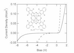
When the current density–voltage characteristics of the PG and VT diodes are measured at room temperature, the PG diode has a larger turn-on voltage and starts to break down at about 8 V reverse bias (see Fig. 1). Its rectification ratio is approximately 104 at 1 V and decreases to about 4 × 10³ at 2 V. On the other hand, the VT diode has a rectification ratio of about 103 at 1 V and breaks down at about 4 V reverse bias.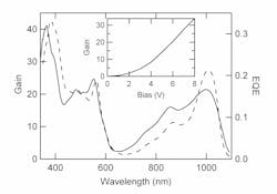

Different diodes, different uses
These two types of diodes are designed for use in different conditions. The PG diodes are essentially photoconductors designed to be used only under significant applied bias. The gain in the structure is produced by circulation of carriers in response to charges trapped in the organic layer(s). This requires charge injection from the contacts in reverse bias to provide the gain. In contrast, the VT diodes are similar to conventional photodiodes designed to be used at zero and small applied bias. The contacts are only required to extract charge from the organic layers.
At zero bias, the difference between these two types of diodes is due to the optoelectronic properties of organic semiconductors and the organic multilayer structures. Organic semiconductors have excitons with large binding energies (from 0.2 to 1 eV) that do not dissociate efficiently at room temperature. Optical absorption in an organic semiconductor produces bound excitons and very little photocurrent since the excitons recombine rather than dissociate. To overcome this problem, organic photodiodes typically employ two organic semiconductors so that excitons created in either semiconductor can dissociate by an energetically favorable charge transfer to the other material. The OSnNcCl2/C60 bilayer performs this role in the VT diode. Excitons created in the OSnNcCl2 layer dissociate by electron transfer to the C60 leaving a hole in the OSnNcCl2. This produces photocurrent due to electron transport in the C60 and hole transport in the OSnNcCl2. The VT diode has relatively high EQE at 0 bias (0.22) because of the efficient exciton dissociation at this interface.
In contrast, the PG diode does not use materials with energy levels that can dissociate the exciton and so the EQE is very small at zero bias (0.01). In this diode, the excitons are dissociated inefficiently either in the OSnNcCl2 layer or at its interfaces, and it performs better without a C60 exciton dissociating layer because C60 has a large ionization potential that reduces hole injection from the cathode required for gain. The VT devices use a thinner layer of OSnNcCl2 to maintain their visible transparency. In both diodes, the BCP functions as an exciton blocking and contact buffer layer.
The photoconductive gain results in the PG diodes are similar to previous observations in organic devices.4, 5 In this process, a fraction of the optically excited excitons dissociate, producing deeply trapped carriers (electrons) and free carriers (holes). If their lifetime is longer than the free carrier transit time, the trapped electrons produce photoconductive gain with a gain per trapped carrier determined by the number of free carriers passing through the device during the lifetime of the trapped carrier.6 The gain (G) of the diode in reverse bias is:
G = χτ/Τ = χτµ(V + Vbi)/L2
Here, χ is the fraction of excitons that dissociate producing trapped and free carriers, τ is the lifetime of the trapped carrier, Τ is the free carrier transit time, V is the applied bias, Vbi is the built-in potential, L is the organic layer thickness, and µ is the free carrier mobility.
In reverse bias, the transit time is determined by the carrier time of flight, Τ = L2µ/µ(V + Vbi), as shown on the right of the gain equation. The built-in potential is about 0.4 V as determined from the zero of photocurrent in forward bias. From the slope of gain as a function of bias (from inset of Fig. 2, >4 V) we determine that χτµ/L2 is approximately 6.5. At zero bias, without photoconductive gain, the quantum efficiency of the PG diode is 0.01, which we take as an estimate for χ. From the frequency dependence of the gain, the lifetime τ is approximately 10-2 s, so the product χτ is 10-4 s. For the diode thickness of 65 nm this corresponds to a hole mobility of approximately 3 × 10⁻⁶ cm2/Vs. This would most likely be a low mobility for pure OSnNcCl2, but this is an average mobility representing transport across the bilayer including BCP. The choice of a constant χτ product is only a simplification; the exciton dissociation fraction has some bias dependence and there is most likely a wide distribution of trapped electron lifetimes.
These two diodes are representative of what can be done with strong IR absorbing, visibly transparent organic semiconductors. A wide variety of gain, quantum efficiency, and transparency combinations are possible. The performance of both diodes can be improved using standard antireflection coatings to increase the external gain and/or diode transparency. Designing organic photodiodes with specific gain and transparency characteristics requires greater understanding of charge transport and trapping in these materials and structures. But these results highlight the potential of the soluble, small molecule OSnNcCl2 for near-IR applications.
REFERENCES
- S.R. Forrest, MRS Bulletin 30, 28 (2005).
- I.H. Campbell and B.K. Crone, Appl. Phys. Lett. 95, 263302 (2009).
- I.H. Campbell, submitted to Appl. Phys. Lett.
- J. Gao and F.A. Hegmann, Appl. Phys. Lett. 93, 223306 (2008).
- I.H. Campbell and B.K. Crone, J. Appl. Phys. 101, 024502 (2007).
- A. Rose, Concepts in Photoconductivity and Allied Problems, Robert E. Krieger Publishing Co., Huntington, NY (1978).
Ian H. Campbell is a research scientist in the Materials Physics and Applications division at Los Alamos National Laboratory, MS D429, Los Alamos, NM 87545; e-mail: [email protected]; www.lanl.gov.