OPTICAL MATERIALS: 'On-silicon' engineered substrates speed photonic device development
"On-silicon" III-V technologies enable an exciting new world where the substrates familiar to the silicon manufacturing industry may be imbued with III-V material properties. Light emission is a key advantage of III-V materials; however, the higher electrical mobility than silicon enables high-speed and high-power electronics applications that are also crucial to the light-emitting diode (LED) lighting industry for the production of voltage regulators and inverters.
Fundamental to any III-V-on-silicon technology platform is that wafers are flat. Flatness can be a challenge when any of the technologically key materials such as gallium nitride (GaN), gallium arsenide (GaAs), indium GaAs (InGaAs), and germanium (Ge) are placed onto silicon (Si) wafers, principally due to thermal expansion issues.
At the high temperatures used in epitaxy, the large differences in thermal expansion coefficients between substrate and layer result in severely bowed wafers upon cooling—so severe in some cases that wafers physically crack. Wafer bow makes it difficult to use standard silicon industry tools such as scanners and steppers to successfully handle the wafers, potentially threatening to eliminate the key benefit of wafer processing using the existing silicon infrastructure; consequently, bow mitigation schemes are of high interest.
At Translucent, we have developed two general approaches for on-silicon technologies depending upon the material system of interest. First, germanium can be deposited directly onto silicon using a modified chemical vapor deposition (CVD) approach. This lends itself well to silicon-substrate-based multijunction solar cell applications as well as GaAs photonic integration applications because it maintains the ability to do front-to-back contacting and therefore does not require rework of device architecture. Our second approach is the use of single-crystal oxide buffer layers. This enables us to fabricate GaN on insulator systems that can be used as substrates for either LEDs or field-effect transistors (FETs) that both currently use top surface contacts.
In addition, the dielectric properties of the oxide can improve the electrical performance of power FETs. Our engineered substrates are suitable templates for metal-organic CVD (MOCVD) growth and subsequent GaN growth has demonstrated properties of light emission. Since a crystalline oxide can support the epitaxy of additional semiconductor layers, it is also possible to embed a distributed Bragg reflector (DBR) within the Si-GaN buffer layer by pairing oxide layers with additional silicon epitaxy.
Ge-on-Si approaches to InGaAs on Si
Translucent has demonstrated Ge epitaxy directly onto silicon substrates without the use of a SiGe composition grading scheme, which is the more common approach within the industry. Our technology uses the addition of tin (Sn) to both control defect propagation and provide binary and ternary alloys with other group IV elements (GeSn, SiGeSn). These films are deposited directly onto silicon using a proprietary high-volume-capable modified CVD route with typical sources being di-germane (Ge2H6), tri-silane, and deuterated tin (SnD4). For our initial product development, we have focused on 5-μm-thick Ge epitaxial layers deposited on silicon as a replacement for the bulk Ge substrates used in high-performance, high-efficiency multijunction solar cells. This requires Sn to be in the 0.1–0.5% range.
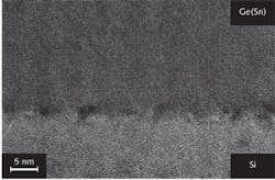
Initial capacitance-voltage measurements indicate that the material is p-type with a carrier concentration of 1 × 1017 cm-3. Roughness measurements indicate that the finished Ge-on-Si template has a root-mean-squared (rms) value of 0.65 nm on a 5-μm-square atomic force microscope (AFM) image—meeting the requirements for subsequent MOCVD epitaxy of III-V materials such as InGaAs. Transmission electron microcopy (TEM) data reveals good crystalline quality and a majority of misfit dislocations pinned at the Ge/Si interface (see Fig. 1). The Ge/Si interface is fairly "clean," which we believe is important for good electrical behavior of this material. Defect analysis via chemical etching indicates defect densities of the order of 1 × 10⁶. X-ray diffraction measurements show that the (004) reflection has a full width half maximum (FWHM) of 0.106° (382 arc-sec), with the Ge exhibiting a tensile strain of 0.17%.
The good growth rates mean that the process lends itself well to high-volume manufacturing. The Ge template can be made up to several microns thick and can act as a starting point for other structures such as multijunction solar cells, GaAs integrated photonics, and potentially laser-based structures. The silicon substrate is chosen so that the Ge has the same crystalline orientation as currently used in bulk substrates; that is, for photovoltaic (PV) templates we grow on Si<100> with a 6° miscut toward the <111> direction. Substrates are boron (B) doped (sheet resistivity of 0.01–0.02 Ω-cm) to facilitate back contacts with current reactors set up to use 100-mm and 150-mm-diameter wafers.
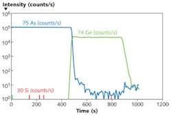
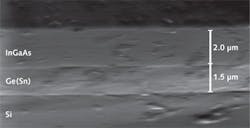
Using Translucent's process, InGaAs films have been grown directly on GeSn by IQE (Cardiff, England). Room-temperature photoluminescence results show a peak photoluminescence at 869 nm, which is expected for the 1–2% In concentration in GaAs (In0.02Ga0.98As) typically grown on Ge in multijunction PV epitaxial structures. Another important metric is to ensure that Ge does not diffuse into the III-V material. Secondary ion mass spectroscopy (SIMS) plots made by IQE indicate that the Ge from the epitaxial layer does not diffuse into the InGaAs, indicating that this material is as stable as bulk Ge (see Figs. 2 and 3).
It is known that varying the Sn concentration in the GeSn layer extends the detection range of Ge into the infrared (IR), enabling some GeSn solar cells to have improved ability to absorb solar radiation.1 Alloying GeSn opens up a path to ternary materials operating at 1 eV—a capability that has long been identified as necessary to push solar cell efficiencies into the 50%+ range. This is an exciting technology because it lays the groundwork for fabricating multijunction solar cells on Si substrates, reducing costs and increasing the possibility of using larger substrates in the concentrated photovoltaic (CPV) solar industry.
SOI approaches to GaN on Si
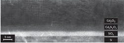
The semiconductor-on-insulator (SOI) approach is a versatile method of achieving on-silicon solutions for lighting and electronics applications. The growth of insulating oxides on silicon is possible because the lattice parameters of several of the binary rare-earth oxides are nearly twice that of silicon. We have developed ways to vary the composition of the oxides; for example, gadolinium neodymium oxide ((Gd1-xNdx)2 O3) where x varies such that the lattice parameter is between 11.08 Å for pure Nd2O3 and 10.81 Å for pure Gd2O3. The lattice constant can be extended by alloying Gd2O3 with erbium oxide (Er2O3) as (Gd(1-x) Erx)2O3. This extends the range to 10.55 Å for pure Er2O3. Carefully controlling the composition of ternary rare-earth oxides can therefore allow very precise lattice engineering such that it matches the lattice parameter of Si.
As already mentioned, bow mitigation is the key to template engineering. Increasing the oxide thickness can produce a wafer with convex curvature able to offset the concave curvature that normally arises from the growth of GaN on silicon. When you add to this that the growth of an oxide from its constituent components (metal and O2) enables both the composition and chemistry of the oxide to be optimized, you have a multifunctional approach to strain engineering. This concept of epitaxial engineering can even be extended to facilitate the growth of an amorphous intermediary layer between the substrate and crystalline upper oxide surface on which to nucleate the GaN (see Fig. 4).
Our virtual GaN substrates are engineered substrates comprising a rare- earth oxide (REO) layer with a seed layer of GaN deposited on top. These engineered substrates are compatible with MOCVD conditions and act as seed layers for subsequent thick GaN layer growth. Detailed studies of XRD linewidth and surface roughness indicate that post MOCVD, both the crystalline quality and the surface roughness improve. Final linewidths are on the order of 600–800 arc-sec (down from approximately 1800 arc-sec), while rms roughness decreases from 8 nm to <1 nm.
Mirrored substrates
On-silicon technologies with the oxide interlayer are versatile tools to achieve lattice matching and strain engineering. However, the material system goes beyond this capability: Distributed Bragg reflectors (DBRs) can be constructed within these dielectric layers to form a reflector. We typically use a material pair consisting of an REO and Si to achieve 85%+ reflectivities (R). Due to the high-index contrast between Si and REO, these high R values can be achieved with only four pairs of layers—significantly better than with other material systems where 10–20 layers are not uncommon.
As with other epitaxial DBR structures, precise control of the layers sets both the center wavelength and the stop band of the DBR (range of wavelength over which R >75%). A typical mirror for LED applications has a center wavelength of 450 nm, a stop band range of 100 nm, and peak reflectivity of 80% or more. We call this our "mirrored-silicon" product, which is suitable for LED lighting designs where the useful light emission is predominantly normal to the surface of the wafer.
For such systems, this technique offers an increase in the available light output for a given LED since photons that propagate toward the substrate are no longer wasted. The benefits depend on the particular packaging scheme used, but when appropriate, this method can potentially increase LED output efficiencies by a comfortable 70% when integrated over useful angles. This material choice is not without issues in that Si does absorb blue light produced by a GaN LED; however, the small number of layers means that R values of 85% are readily achievable.
More SOI progress
Using MOCVD epitaxy on a GaN-on-Si template, we have demonstrated high-power FET structure designs with the benefit of an REO screening layer. The high dielectric constant (high-k) of the oxides means that thinner layers of GaN can be deposited to achieve the same voltage breakdown. These devices enable integration of both light emission and power electronics to drive light-emitting elements on the same substrate. Furthermore, the top layers of III-V and oxide may be etched away, leaving a silicon substrate that could be used for the deposition of silicon electronics circuitry.
GaN-on-Si LEDs offer a potentially attractive alternative to sapphire and a route to wafer sizes of 200 mm and beyond. Financially, this can make sense because fully depreciated Si fabs can be given a new lease on life as GaN-on-Si factories. Fundamentally, the real strength of this technology is that these wafers can be processed in the high-volume, highly automated 150 and 200 mm silicon fabs that are situated across the globe.
We believe that the on-silicon world in which silicon substrates are the basis for III-V electronics and optics is just around the corner. At Translucent, our on-silicon technologies offer both GaN and Ge substrates of interest to the electronics and integrated photonics industries. These materials make Si platforms III-V compatible in a potentially cost-effective and manufacturable environment. We are presently in pilot production and are ramping up our on-silicon manufacturing product lines to accommodate current and next-generation integrated photonic and electronic device needs.
REFERENCE
1. R. Roucka et al., IEEE J. Quantum Electron., 47, 2, 213–222 (2011).
About the Author
David Williams
David Williams is director of photonics engineering at Translucent, a subsidiary of Silex Systems Limited (Palo Alto, CA).
Andrew Clark
Andrew Clark is VP of engineering at Translucent, a subsidiary of Silex Systems Limited (Palo Alto, CA).
Michael Lebby
Michael Lebby is CEO of Lightwave Logic (Englewood, CO).