INTEGRATED PHOTONICS: GaAs modulator is first POET alternative to Si photonics
Scientists and engineers from OPEL Technologies affiliate ODIS Inc. (Shelton, CT) and its research and development center located at the University of Connecticut (Storrs, CT) have developed a high-speed, low-power-consumption gallium arsenide (GaAs)- and aluminum gallium arsenide (AlGaAs)-based optical modulator as part of their Planar Optoelectronic Technology (POET) semiconductor integrated photonics platform.1
Unlike the idea of an end-to-end (laser source to detector) integrated architecture using all-silicon photonic devices and silicon optical interconnects, POET aims for the monolithic integration of III-V semiconductor optical and electronic devices on a single (IC) chip. Modulator development was partially funded by the Air Force Research Laboratory (AFRL) for a POET development contract between ODIS and BAE Systems Reed Microelectronics Center (Nashua, NH).
Better OE integration
Most optical ring-resonator modulators use silicon-on-insulator (SOI) waveguides with silicon dioxide (SiO2) cladding layers; unfortunately, power consumption for these devices can be rather high as absorption depends on the plasma effect in the forward-biased diode.
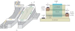
The alternative POET design uses a GaAs/AlGaAs p-i-n quantum-well structure with rectangular waveguide regions to create a blue-shifted modulator that relies on a charge-dependent absorption edge; that is, the absorption change is produced by the blue shift of the band edge in response to the filling of the quantum well (see figure). The device depends critically on the movement of the resonant frequency of the ring during charge injection. The modulation frequency response is determined by the RC circuit response and/or the internal device transit times of the ring structure according to its electrode geometry as well as the optical response of the ring determined by the photon lifetime. Because absorption is across the bandgap and produces electron-hole pairs for every absorbed photon (unlike silicon devices), lower static power levels are needed for control of the quantum well charge. Higher-speed operation is possible because charge removal is facilitated by a high-mobility channel.
The blue-shifted quantum-well structure is also compatible with the fabrication of electronic devices in the same epitaxial structure, and lends itself to easier optical-to-electronic integration with transistor drivers and laser sources.
Modulation performance
The rectangular resonator structure easily accommodates four separate electrical contacts to prevent whispering-gallery modes around its operation wavelength of 850–1000 nm. It also allows fabrication of larger waveguide widths (around 1 µm) than circular resonators to prevent scattering losses that occur when the resonator structure is too close to the waveguides. And finally, the 90º waveguide bends eliminate high-order modes generated in the coupling region.
By carefully optimizing waveguide parameters and subsequent bend efficiency, a resonator with a waveguide width of 1 µm, a gap of 0.25 µm between the waveguide and the resonator, and a rectangular resonator region of 3 × 13 µm shows a normalized output power of 0.7 and 0.04 for input wavelengths of 982.8 nm (resonant) and 985.2 nm (nonresonant), for an extinction ratio of 12.4 dB. Power consumed by the device with a bias voltage of 0.4 V is less than 1 mW.
According to University of Connecticut professor Geoff Taylor, these modulators consume less power and have a higher extinction ratio, smaller footprint, lower voltage, superior bandwidth, and better scalability compared to their SOI counterparts. “A key differentiator is the natural integration of the laser within POET,” says Taylor.
REFERENCE
1. G.W. Taylor et al., 2011 SPIE Optics + Photonics conference, San Diego, CA, paper 8164-11 (Aug. 22, 2011).
About the Author

Gail Overton
Senior Editor (2004-2020)
Gail has more than 30 years of engineering, marketing, product management, and editorial experience in the photonics and optical communications industry. Before joining the staff at Laser Focus World in 2004, she held many product management and product marketing roles in the fiber-optics industry, most notably at Hughes (El Segundo, CA), GTE Labs (Waltham, MA), Corning (Corning, NY), Photon Kinetics (Beaverton, OR), and Newport Corporation (Irvine, CA). During her marketing career, Gail published articles in WDM Solutions and Sensors magazine and traveled internationally to conduct product and sales training. Gail received her BS degree in physics, with an emphasis in optics, from San Diego State University in San Diego, CA in May 1986.