Emissive display shows high-brightness images
Researchers at Canon Inc. (Tokyo, Japan) have developed a new flat-panel cathodoluminescent display based on surface conduction electron emitters (SCEs). The SCE technology promises high brightness, high response, and low cost as well as the potential for large-area displays using conventional cathode-ray-tube (CRT) phosphors. The technology may ultimately provide a strong challenge to plasma displays. One goal of Canon's research is an easy-to-fabricate, 40-in.-diagonal high-definition television screen.
The company has demonstrated a 3.1-in. full-color SCE display for NTSC television signals. The device exhibits very high luminescence—640 cd/m2, which is about six times that of a typical liquid-crystal display (LCD)—at a drive voltage of 13.5 V and anode voltage of 6 kV. The display has 80 × 80 × 3 pixels, and each pixel is 0.72 × 0.23 mm—this is much larger than LCD pixels, but SCEs will not be used as computer displays.
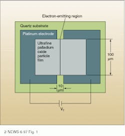
The SCE cathode—the electron-emitting region—consists of a patterned ultrafine-particle (5–10 nm) film of palladium oxide (PdO) dispersed on a pair of patterned platinum electrodes mounted on a quartz substrate (see Fig. 1). The nanostructure of the SCE required control of several parameters, including the diameter of the ultrafine particles, the thickness of the film, and its resistance.
The SCE display comprises SCE cathodes and a high-voltage anode with conventional CRT phosphors. The anode and cathode regions are separated by a vacuum space (see Fig. 2). Electrons emitted from the SCEs are accelerated by an electric field and make the phosphors emit red, green, and blue. The SCEs, which are arranged as a matrix, are electrically connected to row lines and column lines on the cathode plate. The SCE cathodes emit electrons at an operating voltage of about 14 V, and there is no emission at half the operating voltage of 7 V. The low drive voltage eliminates the need for electron-beam focusing to make suitable luminescent patterns of phosphors, thus simplifying the whole architecture.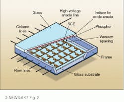
According to Canon, newly developed field-emission displays (FEDs) exhibit several disadvantages compared to SCE displays. First, FED fabrication needs fine-resolution semiconductor-manufacturing equipment. Second, the drive voltage for FEDs is rather high (about 50 V) because the distance between gates and emitter tips is more than submicron. And, as for the architecture, with a high-voltage anode over a several-millimeter-scale vacuum spacing, the high gate voltage spreads the electron beam, resulting in large luminescent patterns on phosphors. Electron-beam focusing methods are, therefore, required to narrow the luminescent patterns.
Problems that must be solved to commercialize the SCE display include how to sputter the ultrafine particles over substrates of 40-in. diagonal or more and how to provide support or frames for the vacuum covering that will not interfere with the pixel continuity of the display—these supports must be less than the pitch of two pixels.
The display was described at the third International Display Workshop (Kobe, Japan) held last November. Interestingly, when Canon researchers were asked about properties of the 5- to 10-nm particles in the electrode-emitting region of the SCE cathode or for a model for electron emission within the SCE cathode, they said they did not know. Few in the audience, however, seemed to believe that. And mechanisms will likely be expounded in a later paper to be published in 1997.