Ultrafast photoacoustics enables optical diagnostics of opaque materials
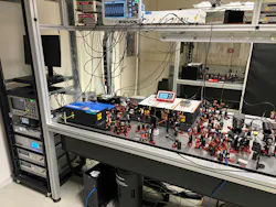
In an advance for photonics, a group of researchers from Delft University, the Advanced Research Center for Nanolithography, and ASML Research in The Netherlands recently had a little fun with physics and created an optical metrology approach that listens with light and sees sound to achieve nanometer-level alignment metrology through optically opaque layers.
A key part of manufacturing integrated circuits (ICs) involves lithography and wafer alignment. And while optical methods are fast and noninvasive, the increasing use of optically opaque materials makes optical metrology more complex on markers within deeper layers.
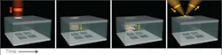
The researchers’ approach taps an ultrashort (picosecond) light pulse to generate ultrasound within the optically opaque layer, which propagates to the imaging target below. This ultrasound pulse bounces off the target, and its reflection can be detected at the top of the opaque material by another light pulse.
While the group has used this trick before, now they’ve demonstrated it on an alignment grating covered with a 1.3-µm-thick layer of amorphous carbon—and achieved 15-nm positioning reproducibility within 1 second. More good news: It shows potential for further scaling.
It’s an advance for photonics because “it significantly expands the application range of optical metrology by enabling all-optical measurements through optically opaque materials,” says Stefan Witte, a professor of optics for nanoscale metrology at Delft University. “For many applications, including semiconductor metrology, the speed and noninvasive, noncontact nature of optical measurements are essential.”
Witte and colleagues view the optics and imaging science field as an enabling technology. “It provides the tools for many applications in science and industry,” Witte says. “The semiconductor industry is one application area in which optics is really pushed to its limits to make smaller and more intricate electronics. It’s an exciting field to be in, and we collaborate with industry on various projects related to metrology tools for positioning and characterization—this work is the result of such a collaboration.”
Visualize microscopic structures covered by optically opaque materials
The main measurement concepts behind the group’s approach involve ultrafast pump-probe spectroscopy and point-scanning microscopy. “We wanted to create an optical measurement method to allow visualization of microscopic structures covered by layers of optically opaque materials,” says Witte. “And the main physics concept involved is ultrafast heating. The pump pulse is absorbed by the opaque material, which causes a rapid temperature increase of a thin layer at the surface. This rapid heating causes stress, which results in the formation of a rapid expansion/strain wave—it’s effectively an ultrasound pulse that propagates into the structure and can reflect from the structures and interfaces it encounters.”
When such a reflected strain pulse returns to the surface, “it transiently changes optical properties such as reflectivity,” he explains. “By measuring this reflectivity with a time-delayed probe pulse, we can detect the ultrasound pulses. Our approach can be used as an imaging tool by tightly focusing pump and probe spots and performing consecutive measurements at different positions across a sample.”
What does the setup involve?
The group’s setup is a pair of modelocked femtosecond fiber lasers from Menlo Systems—a Yb-doped fiber laser at 1030-nm wavelength as the pump, and a frequency-doubled Er-doped fiber laser at 780 nm as the probe. “For time-resolved measurements, we electronically synchronize these lasers to control their relative pulse repetition frequencies,” says Witte. “This approach is known as asynchronous optical sampling (ASOPS) and it makes the time scanning fast and stable.”
For measurements, the researchers use the pump pulse to launch an ultrasound pulse into a sample, and then record the probe pulse reflectivity as a function of the pump-probe time delay. “Any ultrasound reflections from hidden features inside the sample are detected as rapid transient reflectivity changes, in which the time delay encodes the depth of such a hidden feature,” he points out. “By performing such measurements while also scanning the laser spots across the surface, we can record a spatial map of the hidden features.”
For more practical metrology, scanning across a known grating-like target, “we actually fix the pump-probe delay to the correct timing and do a spatial scan across the target to ‘see’ the grating lines. So you can say we’re actually listening with light—or seeing the sound,” Witte says.
Spatial resolution limited by optics, not acoustics
One particularly surprising aspect they discovered is that spatial resolution is still limited by the optics, but not at all by the acoustics. “Usually ultrasound is associated with much lower resolution than optics because the wavelength of sound is so much larger,” he says. “But the ultrasound we generate with femtosecond laser pulses has extremely high frequencies, in many cases above 100 GHz.”
The resulting wavelength is much shorter than the wavelength of light, and the acoustic propagation doesn’t degrade the spatial resolution with which the metrology targets can be imaged. “Aside from imaging through hard mask materials such as amorphous carbon, we’re using this method to image through layers of aluminum and gold,” he says. “It’s like looking through a mirror, which is cool.”
Challenges left to overcome? “In the end, it’s about how fast you can detect an acoustic signal with sufficient signal-to-noise ratio (SNR), because it limits how accurately the position of the metrology target can be determined,” says Witte. “The relative reflectivity changes we detected from the carbon layers using our experimental parameters were within the range of 10-5, so very small. From such signals we can retrieve the target position with 14-nm accuracy within 1 second of measurement time.”
Sounds good, right? But semiconductor wafer alignment “is typically done with ~1-nm precision and much faster,” he adds. “Meeting industry requirements will require more work—both increasing the measured signals and faster measurement methods.”
The researchers’ work may enable optical semiconductor metrology whenever opaque materials are involved, but it also shows potential for other materials processing and characterization areas as well because it enables optical diagnostics of opaque materials.
Next up, the group plans to “explore ways to increase the sensitivity to detect the ultrasound, and possibly ways to generate stronger ultrasound pulses by tailoring the optical pulse parameters,” says Witte. “Beyond continuing this work on metrology, we’ll also explore the potential of our approach for 3D imaging inside opaque nanostructures. This work is the final achievement of Matthijis Velsink’s Ph.D. research, and his thesis will be available soon with more information.”
FURTHER READING
M. Velsink, M. Illienko, I. Setija, and S. Witte, Light: Adv. Manuf., 7, 3, 835–843 (2026); https://doi.org/10.37188/lam.2026.083.
About the Author
 Sally Cole Johnson
Editor in Chief
Sally Cole Johnson is Laser Focus World’s editor in chief, and she has more than 25 years’ experience as a science and technology journalist. She specializes in physics and semiconductors, and wrote for the American Institute of Physics for more than 15 years, and also covered theoretical physics and neuroscience for the Kavli Foundation, and complexity for the Santa Fe Institute. Johnson has also written extensively about military embedded systems, high-performance computing, software-defined networks, and infosec. She is a member of the National Association of Science Writers (since 2001).
When she isn’t writing about optics, photonics, or quantum advances, you can find her outside in northern NH in the garden with birds landing in her hand or heading for the mountains with her bike, skis, or crampons and ice axe.
Related
 Photoacoustic Microscopy

