Six-axis stage advances optical probing of wafers
Planar manufacturing and test of optical components is still in its infancy but recent developments may enable routine wafer-level probing of optoelectronic devices
Wafer-based probing of semiconductor chips during manufacture is an established technique used extensively across the semiconductor industry. The information it yields is of primary importance to efficient manufacturing, enabling higher yields, improved process monitoring, early fault detection, and so on.
Although optical-component manufacturing technologies have now reached the point at which many planar devices are competitive with their discrete micro-optical counterparts—most notably arrayed-waveguide-grating (AWG) devices for dense-WDM filtering and switching—wafer-based probing of optical products is still in its infancy. It should not be overlooked that wafer-based optical probing is applicable to all heterojunction lasers and detectors, and it will be a crucial tool for the winners of the next wave of optical-component manufacturing.
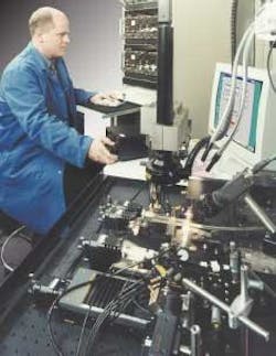
With the exception of vertical-cavity lasers, the most efficient optical probing of devices to date has been achieved by sawing wafers into bars, then polishing or even coating the optical facets before placing them in some form of test rig that is capable of scanning through each device within the bar (see Fig. 1). This form of testing is very inefficient compared to wafer-based probing because of all the intermediate processing steps (value added) and the constraints involved when handling the materials.
Breaking down the barriers
Because of the potential for high-volume cost-efficient manufacturing, overcoming the barriers to optical wafer-based probing is something that should be of keen interest to every optical-component manufacturer. There are three key reasons why optical probing of wafers has not been achieved to date: the inability of wafer materials processing to provide optical access to devices (with the exception of vertical-cavity lasers), the lack of suitable optical probes, and lack of automatic alignment compatible with existing wafer-probing systems. In fact, we can now demonstrate solutions to each of these barriers.
Optical access. The newest wafer-fabrication techniques are capable of etching narrow channels into wafers. These channels can be deep enough to allow limited optical access to the facets of the optical devices on the wafer (lasers, detectors, modulators, switches, AWGs, and so on) and the quality of the optical facets is sufficiently high so as not to detract from device performance.
Echelle gratings, AWGs, and other passive optical circuits are typically made using silica-on-silicon technology. Other material systems can also be used, such as indium phosphide or polymers, but these materials present some challenges in coupling and propagation losses. Silica-on-silicon processing involves deposition of very high-quality silica (SiO2) onto a silicon substrate, with the optical waveguides being etched in a core layer, typically doped with germanium or phosphorous.
The waveguides usually have dimensions of 6 × 6 µm, creating a waveguide mode that is extremely well matched to that of standard single-mode optical fiber. A thick cladding layer is deposited over the etched waveguides to provide the optical confinement and isolate the waveguide core from any surface or environmental contaminants. To provide access to this waveguide core for optical-probing purposes, a deep trench of approximately 30-µm depth and less than 100-µm width must be etched through this top cladding. These trenches are narrower than the blades of most wafer-dicing saws, which means they can sit passively in the dicing frames and not contribute to any increase in device size or complexity.
In the past, an etch process of this depth, with suitably high-quality facets was not readily available. However, most modern wafer-fabrication facilities now use inductively coupled plasma reactors or another form of advanced oxide etcher, and are fully capable of manufacturing this trench with nearly 100% yield across a full 8-in. wafer. This development has allowed new automated optical-probe systems to operate on every die across a 6- or 8-in. wafer.
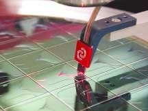
Optical probes. The latest commercially available optical probes are capable of operating within narrow wafer etched channels (see Fig. 2) and this newer type of probe overcomes the issues associated with achieving optical access within a narrow channel, while simultaneously providing single-mode light propagation.
Such a probe can be customized to nearly any mode size required for the wafer material system. These sizes typically range between 2 to 10 µm-square but nearly any size can be accommodated. Furthermore, because all the probe tips (which couple the light from the probe into the waveguides) are defined lithographically, an array of waveguide probes can be created at nearly any pitch. This allows for fully automated testing of components like demultiplexers, which typically have 8 to 40 channels, and allows all these channels to be tested simultaneously. A multichannel probe obviously requires optical alignment in an additional plane to ensure that all channels are coupled appropriately, but this is a standard process in optical-device assembly. The ability to do it in a fully automated fashion, with rapid alignment and active feedback to constantly track and optimize this coupling, is a more recent development that has been another enabling technology for on-wafer optical testing.
Most recently, wafer probes have been demonstrated with insertion losses of less than 2 dB. This value is typically calibrated out of any device measurements and is not an issue. The polarization-dependent loss (PDL) of these probes is usually less than 0.5 dB, and once referenced appropriately, it can also be calibrated out of most measurements. These probes are intended for very high-volume, high-speed testing at the wafer level, usually for prescreening of die. This prescreening permits only functional components to proceed to full device testing, one of the most expensive aspects of optical-component manufacturing. The performance specifications noted above are more than sufficient to accomplish the rapid prescreening and are now even approaching the level of full device testing performance.
Alignment. Automated nanopositioning of optical probes with respect to the devices on the wafer is the final technological hurdle to making optical wafer probing a reality. Depending on the process, somewhere between four and .
six axes of precise control of the optical probe are needed. To obtain optimal coupling from a probe to small (2-µm) waveguides, a positioning resolution of around 10 nm is needed. So the final challenge comes in the form of providing a six-axis nanopositioning mechanism compatible with a traditional wafer-probing station and capable of rapidly and repeatedly aligning to devices.
In this respect, differentiation needs to be made between techniques of "active alignment," which is nanopositioning based on feedback derived from the coupled signal, and "numerical alignment," whereby nanopositioning is based on mapping—in software—the coupled signal, then analyzing the map and deciding at which location maximal coupling is achieved.
Under the constraint of minimal alignment time and maximal post-alignment stability, active techniques can be regarded as the more suited, though they do require more careful initial setup. This initial setup time is quickly "repaid" because of the high number of like devices that will be aligned.
Active systems generally use piezoelectric actuators to move rapidly over small distances (less than 20 µm). Such actuators are far more efficient at repeated small moves than using precision DC or stepper motors.
Regardless of whether active or numerical alignment techniques are used, the final constraint involves using a set of precision electromechanical tools in conjunction with a wafer-probing system—a limitation that eliminates the vast majority of currently available solutions. Nonetheless, we have recently introduced a nanopositioning stage that provides the necessary six degrees of freedom and precision motion control within a space envelope that allows the positioner to reside on the standard platen of a wafer-probe station (see Fig. 3).
Integration
It is one thing to recognize that the individual constraints to wafer-based optical probing can be overcome, but bringing them together into a viable manufacturing solution provides another set of challenges. Central to the integration process is the wafer-probe station. By starting with a system that already caters to the needs of semiconductor processing, the gains of throughput and reliability can be immediately transferred to photonics manufacturing.
Hardware integration involves mounting the six-axis stage onto the platen of the wafer-probe station and mounting the optical probe appropriately. This simple hardware integration is appropriate for devices such as lasers and detectors with only a single input or output port. For devices such as modulators, AWGs or any multiport optical device, a second six-axis stage must be mounted onto the platen. In these instances the optical probe may need to be a multichannel device.
The final integration step involves the software—critical to any integrated manufacturing system—which must coordinate all the motion control of the wafer station, motion control of the nanopositioning stage, and log all requisite data from optical characterization instruments.
Operation
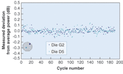
Successful operation of an integrated system requires an initial calibration of all its elements—the wafer chuck, six-axis nanopositioner, instrumentation, and so on. Thereafter, a wafer containing many hundreds of devices can be placed into the probe station, which can then—with full automation—align, optimize coupling, and characterize every device on the wafer. Device throughput and characterization repeatability need to be of the highest level (see Fig. 4).
This repeatability in the insertion loss of a planar device is on par with more traditional measurement techniques, yet can be performed fully automated across a full wafer with little to no user intervention. When measured using modern optical test equipment with full vector analysis, this probe system can easily measure a typical waveguide device in approximately 1 to 2 seconds. The time required for the probe station to move to another die and perform the full six-axis alignment is also approximately 1 to 2 seconds. This is a dramatic advance from the more conventional manual testing approaches, which can easily exceed 10 minutes for a comparable alignment, test, and remounting of a single device.
STEVE KIDD is general manager of Melles Griot U.K., 1 St. Thomas Place, Ely, England; e-mail: [email protected]. MATT PEARSON is director of technology development and BOUMY SAYAVONG is a senior engineer at LNL Optenia, 400 March Road, Ottawa, Canada; e-mail: [email protected] and [email protected].


