Materials beyond silicon: The industrial push for advanced integrated photonics

A modulator remains the most strategically important component on a photonic integrated circuit (PIC). Depending on their design, modulators control either the amplitude or the phase of light, and phase modulators often enable complex multilevel encoding schemes. Most devices fall into one of three categories: Simple waveguide phase shifters, resonant ring structures, or Mach-Zehnder interferometers. Each approach balances different tradeoffs in size, efficiency, and manufacturability.
At the heart of modulation lies the material itself. Some devices rely on phase-change materials, switching between transmissive and opaque states through metal-to-insulator transitions. Others exploit carrier modulation, in which electrical bias alters the refractive index by injecting or depleting charge carriers. The most promising mechanisms for high-speed operation are electro-optic effects—the Pockels and Kerr effects—in which an electric field directly changes the refractive index of the material.
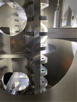
This pursuit is driven by the maturation of silicon photonics. During the past few years, chipmakers reached integration levels of more than 10,000 optical components per chip, which pushed the field into scaling comparable to the evolution of electronics in the 1970s. As production scales, wafer size becomes critical. Although 150-mm wafers served early R&D, Intel is shifting to 200-mm platforms to achieve volume manufacturing economics, and the recent sale of Intel’s photonics division to Jabil underscores that the market is crossing from research scale into mass production.
Modulator material choices
The choice of modulator materials has become a defining competitive factor. A 2023 review ranked candidates by both performance and complementary metal-oxide semiconductor (CMOS) compatibility.1 Silicon remains the easiest to integrate, but demands high power due to its reliance on thermal effects. Ferroelectric materials—lithium niobate (LiNbO3), barium titanate (BaTiO3), and ferroelectric polymers—offer true electro-optic modulation, but pose fabrication challenges. LiNbO3 delivers superb bandwidth and low loss, but devices are physically large and lithium contamination is problematic for silicon fabs. BaTiO3 promises record-high modulation efficiency, but is still under development. Polymers are flexible and fast, but degrade above 80°C and must be hermetically sealed.
The market, while modest in volume, is growing rapidly. LiNbO3 modulators are projected to reach $1.2B by 2033,2 at an annual growth rate of more than 40%. This surge reflects the limits of conventional silicon solutions. Silicon modulators based on thermo-optic or plasma dispersion effects are reliable, but slow and power-hungry. Data center traffic, artificial intelligence (AI) workloads, and next-generation optical interconnects demand devices that combine low drive voltage (Vπ < 3.5 V), minimal loss, and bandwidths extending into the tens of gigahertz. Silicon struggles to hit these targets.
This is where LiNbO3 and BaTiO3 stand out. LiNbO3’s r33 coefficient (~35 pm/V) supports terahertz-class performance, while BaTiO3’s enormous coefficient (~1300 pm/V in bulk) enables strong modulation for short distances. The latter’s effect stems mainly from optical phonon and strain contributions, which give it high efficiency even at low temperatures. Integration with silicon typically involves a strontium titanate (SrTiO3) buffer layer to manage lattice mismatch, with deposition achieved via molecular beam epitaxy (MBE) or sputtering. Recent demonstrations show monocrystalline BaTiO3 films with excellent uniformity across 200- and 300-mm wafers, achieving Pockels coefficients near 1000 pm/V.
Industry advances
Device performance is advancing rapidly. Academic and industrial groups have reported ring resonators and Mach-Zehnder interferometers in BaTiO3 with optical quality factors up to one million and propagation losses as low as 0.14 dB/cm. It rivals mature LiNbO3 technology, achieved without wafer-scale poling. As these films transition from laboratory prototypes to foundry-ready platforms, BaTiO3 is one of the few materials to combine high speed, high efficiency, and CMOS compatibility.
The outlook for modulators is similar to early transistors with multiple competing materials. LiNbO3 will likely dominate high-performance telecom and data center links. BaTiO3 may lead in compact, energy-efficient on-chip applications. Silicon will remain essential for co-integration and low-cost scaling. The companies mastering heterogeneous integration across these materials—on 200 mm and beyond—will define the next era of large-scale photonic integration.
La Luce Cristallina
Texas startup La Luce Cristallina (La Luce) is pioneering the integration of BaTiO3 (BTO) with silicon, which ushers in a new era for electro-optic technologies. The company builds on decades of research that began at Motorola Labs, where scientists explored perovskite integration for advanced transistor gate stacks.
La Luce became the world’s first supplier of silicon-integrated BTO wafers in 2023 by offering 2-inch BTO-on-silicon (BTO-on-Si) and BTO-on-SOI (silicon-on-insulator) products. The company also launched an 8-inch wafer facility, with initial production expected by Q1 2026. BTO’s exceptional electro-optic properties—up to 900 pm/V in thin films on silicon—combined with low waveguide losses (~0.1 dB/cm), CMOS compatibility, and operation at 300 GHz, make it an ideal platform for Mach-Zehnder interferometers, ring resonators, LiDAR, and optical computing.
Despite its promise, widespread adoption faces challenges, notably the absence of foundry-ready processing and photonic design kits (PDKs). La Luce is actively collaborating with foundries and equipment makers to bridge this gap, positioning BTO-on-Si as a cornerstone for next-generation photonics.
CCraft
Swiss startup CCraft was spun out from the Swiss Centre for Electronics and Microtechnology (CSEM) and is emerging as one of the first dedicated foundries for thin-film LiNbO3 (TFLN) photonic chips. Owning its facility allows full control over process recipes—a critical advantage for protecting intellectual property and ensuring flexibility in a rapidly evolving field.
During four years of pre-commercial collaboration at CSEM, CCraft refined its understanding of customer needs across datacom, telecom, space, and quantum applications. The verdict: No single material satisfies all photonic functions but for ultrafast modulation and frequency conversion, LiNbO3 is unmatched. Until now, the market lacked a commercial foundry that could deliver TFLN devices with the reliability and volume demanded by industry. CCraft intends to close this gap.
Operating from a certified fab in Neuchâtel and expanding to a larger site within the region, CCraft is building an industrial-grade TFLN platform targeting production capacity of up to 20,000 wafers (200-mm) per year within four years.
CCraft also addresses the growing need for hybrid integration. Its high-yield process produces wafers with up to 10,000 TFLN chiplets for micro-transfer printing onto silicon photonics to support heterogeneous integration and backend processing for bonded dies. This flexibility positions the company as a key supplier to enhance silicon photonics platforms struggling to meet next-generation bandwidth and efficiency requirements.
Aluvia Photonics
Founded in 2022 as a spinoff from the University of Twente, Aluvia Photonics pioneers PICs based on aluminum oxide (Al2O3)—a material poised to fill one of the last major gaps within the photonics spectrum.
Unlike indium phosphide, silicon, or silicon nitride (Si3N4) platforms, Al2O3 offers an exceptionally wide transparency window that extends from the deep ultraviolet (~200 nm) to the mid-infrared. It’s uniquely suitable for ultraviolet (UV) photonics, which is an area where existing materials fall short. Aluvia Photonics has demonstrated propagation losses as low as 1–5 dB/m within the telecom band and ~1 dB/cm at 405 nm—setting new benchmarks for low-loss UV operation.
Beyond transparency, Al2O3 can be doped with rare-earth ions to enable active functionality. Erbium-doped devices have achieved ~25-dB fiber-to-fiber net gain, 50-mW output power, and 6-dB noise figures—metrics on par with erbium-doped fiber amplifiers but at a fraction of the size and cost. Thulium-doped devices have produced watt-level continuous-wave outputs and high-peak-power pulse amplification. The platform also has high linearity and power handling, which is ideal for data center and telecom systems that demand signal fidelity.
Aluvia Photonics’ CMOS-process-compatible Al2O3 platform merges the compactness of semiconductor amplifiers with the performance of fiber systems. By extending integrated photonics into the UV and offering active, scalable solutions, the company stands ready to redefine the material foundations of next-generation PICs.
SCIA Systems
Germany-based SCIA Systems makes thin-film process equipment for advanced micro- and nanotechnologies and is applying its expertise in ion beam and plasma technologies to PICs.
For photonics manufacturing, wafer-level performance depends critically on film thickness uniformity and structural precision. SCIA Systems addresses both through two complementary processes: Ion beam trimming and reactive ion beam etching. Ion beam trimming enables sub-nanometer correction of film thickness on 200-mm wafers, which reduces variation from several nanometers to just 0.1-nm root mean square (RMS) roughness.
To refine waveguide geometry, SCIA uses reactive ion beam etching. A focused ion beam cleanly sculpts features with sidewall angles above 75° and sub-nanometer roughness. The process avoids redeposition and damage—even when working with sensitive photoresists or complex multilayer stacks.
SCIA Systems enables the precision control required for high-performance waveguides in materials such as LiNbO3, aluminum nitride (AlN), and Al2O3. Its ion-beam technologies deliver the uniformity, structural fidelity, and yield essential for scaling integrated photonics to industrial production—and it makes SCIA Systems a key enabler within the photonics manufacturing value chain.
Leybold Optics
As PICs advance toward larger wafer formats and tighter performance tolerances, Leybold Optics provides precision surface treatment that bridges optical and semiconductor manufacturing. The company’s ion beam trimming (IBT) and magnetron sputtering technologies enable ultra-uniform, low-loss photonic layers across Si3N4, LiNbO3, and Al2O3 platforms.
Leybold’s 200- and 300-mm systems complement traditional CMP by performing the final planarization step that defines device yield. Ion beam trimming reduces total thickness variation to less than 5 nm and micro-roughness from 0.5 to 0.2 nm to ensure consistent optical properties across the wafer.
Leybold’s magnetron sputtering tools deposit hydrogen-free Si3N4 layers—essential for low-loss waveguides at 1.55 µm and compatible with semiconductor-grade temperature limits. The company collaborates with partners across the photonic ecosystem to qualify these processes for large-scale production.
Along with the materials advances from Aluvia Photonics, CCraft, and SCIA Systems, Leybold Optics completes a critical link in the value chain by delivering the surface precision that turns innovative materials into manufacturable photonic devices.
Recognizing that most material platforms lack native lasing capability, the company developed hybrid laser modules with external gain sections that can be adapted to multiple technologies—including silicon photonics, Si3N4, and Al2O3, the latter in partnership with Aluvia Photonics. These hybrid sources can be tested as standalone evaluation modules or combined with foundry-fabricated circuits, which gives designers a practical route to validate performance before committing to full wafer runs.
By combining multiplatform design expertise with ready-to-integrate laser solutions, the company closes one of the final functional gaps within the PIC ecosystem—and it complements the manufacturing advances of CCraft, SCIA Systems, Aluvia, and Leybold Optics to bring photonic integration closer to industrial maturity.
In conclusion, the field of PICs is undergoing a profound transformation, moving beyond the limitations of silicon. The rise of specialized materials like thin-film lithium niobate, barium titanate, and aluminum oxide is enabling unprecedented performance in speed, energy efficiency, and spectrum of operation. This material revolution, supported by advances in precision manufacturing and cross-platform design, is forging a new, heterogeneous ecosystem. As these technologies mature and scale on larger wafers, they are collectively pushing integrated photonics from specialized research into a new era of industrial-scale production and commercial success.
REFERENCES
1. A. A. Demkov and A. B. Posadas, IEEE J. Sel. Top. Quantum Electron., 30, 8200113 (2024).
2. See www.verifiedmarketreports.com/product/lithium-niobate-ln-modulators-market.
About the Author

Ivan Nikitski
Dr. Ivan Nikitski serves as a Photonics Technology Expert at EPIC, the European Photonics Industry Consortium, which stands as the world's largest association of photonics companies with over 800 corporate members. Ivan earned his Ph.D. with honors in photonics from ICFO, the Institute of Photonic Sciences. After successfully transitioning to an expert role in the semiconductor industry in France, he now provides a special blend of academic and industrial views on integrated photonics, optoelectronics, advanced materials, and quantum technologies.