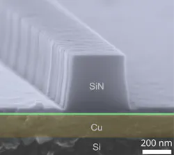
Researchers from the Moscow Institute of Physics and Technology (MIPT; Moscow, Russia) have shown that copper nanophotonic components can operate successfully in photonic devices;1 it was previously believed that only gold and silver components had the required properties for this. This means that light-based computers are closer to reality than before, as copper is cheaper than gold or silver; in addition, copper components can easily be implemented in integrated circuits using industry-standard CMOS fabrication processes.
These studies also provide a foundation for the practical use of copper nanophotonic and plasmonic components, which in the very near future will be used to create LEDs, nanolasers, highly sensitive sensors and transducers for mobile devices, and high-performance optoelectronic processors with several tens of thousands of cores for graphics cards, personal computers, and supercomputers.
Why plasmonics?
The diffraction of light limits the minimum dimensions of photonic components to the size of about a wavelength (~1 μm). Despite the fundamental nature of the diffraction limit, one can overcome it by using metal-dielectric structures to create truly nanoscale photonic components. Most metals show a negative permittivity at optical frequencies and light cannot propagate through them, penetrating to a depth of only 25 nm. But light can be converted into surface plasmon polaritons — waves propagating along the surface of a metal. This makes it possible to switch from conventional 3D photonics to 2D surface plasmon photonics, or plasmonics, allowing the control of light at a scale on the order of 100 nm, far beyond the diffraction limit.
Experimental fabrication achieved
In 2012 the MIPT researchers found that copper as an optical material is not only able to compete with gold, but it can also be a better alternative. Unlike gold, copper can be easily structured using wet or dry etching, allowing nanoscale components to be easily integrated into silicon photonic or electronic integrated circuits. It took more than two years to set up and confirm this hypothesis experimentally. “As a result, we succeeded in fabricating copper chips with optical properties that are in no way inferior to gold-based chips,” says the research leader Dmitry Fedyanin.
The researchers note that the optical properties of thin polycrystalline copper films are determined by their internal structure and the ability to control this structure; achieving and consistently reproducing the required parameters in technological cycles is the most difficult task. “We conducted ellipsometry of the copper films and then confirmed these results using near-field scanning optical microscopy of the nanostructures,” says Fedyanin. “This proves that the properties of copper are not impaired during the whole process of manufacturing nanoscale plasmonic components.”
Source: MIPT
REFERENCE:
1. Dmitry Yu. Fedyanin et al., Nano Letters, publication date (Web): December 14, 2015; doi: 10.1021/acs.nanolett.5b03942
About the Author
John Wallace
Senior Technical Editor (1998-2022)
John Wallace was with Laser Focus World for nearly 25 years, retiring in late June 2022. He obtained a bachelor's degree in mechanical engineering and physics at Rutgers University and a master's in optical engineering at the University of Rochester. Before becoming an editor, John worked as an engineer at RCA, Exxon, Eastman Kodak, and GCA Corporation.

