Researchers at the Istituto Elettrotecnico Nazionale Galileo Ferraris (IEN; Turin, Italy) have fabricated and patterned porous silicon to provide lateral waveguide confinement while at the same time leaving a flat surface on which further circuitry can be deposited. The technique uses localized oxidation and collapse caused by exposure to a focused laser beam. The structures produced operate as they were designed to—as single-mode waveguides—and have, according to initial experiments, a loss of less than 1 dB/cm.
Porous silicon has the property that its refractive index varies widely depending on the level of porosity. The problem with the material has been that it is not easy to pattern porous silicon photolithographically; in addition, the resulting waveguides would take up space that could be used for other purposes. The approach at IEN has been, instead, to make sections of the silicon substrate itself porous in the form of a plane that guides vertically, and then to use a laser technique to provide the lateral confinement.
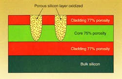
To achieve this, the researchers first created porous silicon layers of different refractive index to act as the waveguide top cladding, core, and bottom cladding. This was done first by removing the parasitic surface layer of a crystal of p+-type <100> single polished silicon and then anodizing the substrate underneath. They then used an electrochemical cell with a hydrofluoric-acid:ethanol solution to make the silicon porous. For the top cladding layer (1.18 µm thick, porosity 77%), current at a density of 440 mA/cm2 was applied for 4 s in 0.2-s steps; in between the steps, an etch-stop bath was used for 10 s, allowing the solution inside the pores to be replenished. The core (3.8 µm thick, 75% porosity) and bottom cladding layer (8 µm thick) were made using essentially the same process.
Once the waveguiding slab has been created, the waveguide is patterned using a 488-nm argon-ion laser beam focused down to a 10-µm spot. The substrate is moved relative to the spot to allow the desired pattern to be imparted. During this procedure—called laser local oxidation (LALOX)—the local temperature reaches 900°C, producing two different effects. Near the surface, which is exposed to air, the silicon forms an oxide and so is strengthened. Beneath the surface, however, the porous silicon cannot withstand the high temperature and collapses. Both processes perform the main necessary function, which is to produce a sufficiently large refractive-index change to allow light to be guided (see figure).
For structural integrity, it would be ideal to have the porous silicon also oxidized below the surface. This could be done using a preoxidation step, where the material is heated to 350°C in oxygen. Then, after LALOX, the resulting structures would contain an oxide skeleton, allowing the resulting structure to undergo further high-temperature processes. However, in their experiments, the IEN team did not attempt to use this technique because they wanted to avoid introducing unnecessary refractive-index changes.
Despite cleaved facets providing a lossy input to the waveguides, and mismatch between the size of the fabricated waveguides and input fibers, researchers were able to do some qualitative experiments on the waveguide quality. They found that the guiding structures themselves were very efficient: a 12-dB loss was measured over distances of both 1 mm and 1 cm (any difference was undetectable with their equipment), suggesting that the input coupling, rather than absorption in the waveguide, was the cause of loss. Also, despite the fact that the lateral confinement channels did not penetrate the full depth of the cladding, only single-mode propagation was detected—an observation that was backed up by theoretical calculations.
REFERENCE
- Andrea M. Rossi et al., Appl. Phys. Lett. 78 (20), 3003 (May 14, 2001).
About the Author
Sunny Bains
Contributing Editor
Sunny Bains is a contributing editor for Laser Focus World and a technical journalist based in London, England.