'In-chip' devices enable truly 3D silicon photonics
Much progress has been made in fabricating on-chip silicon devices in a two-dimensional (2D) plane. Now, researchers at Bilkent University and Middle East Technical University (both in Ankara, Turkey), in collaboration with colleagues in Germany and the U.S., have fabricated "in-chip" microstructures and photonic devices deep within silicon using nonlinear laser lithography that enable dense, truly 3D silicon photonics.
The fabrication technique may seem similar to pre-existing methods for fabricating volumetric holographic gratings and "in-glass" microstructures similar to the European Union's Femtoprint project, but instead achieves the same feat in silicon by exploiting nonlinear feedback mechanisms in the laser-material interaction. The researchers use a custom-made nanosecond-pulsed fiber laser emitting at a 1550 nm wavelength (where silicon is transparent) focused to create two counterpropagating beams to controllably create fine features with dimensions on the order of 1 μm at any depth within bulk silicon.
Self-organization vs. point-by-point processing
Each pulse of the fiber laser leads to a well-controlled light-matter interaction that causes beam collapse followed by permanent modification of the crystalline structure in a roughly 1 μm volume (see figure). This enables the fabrication of 3D structures--however, there is a catch.
Considering a simple real-life application requiring a 10 mm volume, processing with 1 μm points would mean 10 point-by-point steps, requiring unfeasible processing times. To circumvent this limitation, the researchers realized that most structures can be divided into rod- or needle-like subcomponents of 1 μm width, but elongated hundreds of microns along the laser propagation direction-building blocks that can be rapidly assembled.
To create the rod structures, competing effects of thermal nonlinearity and free-carrier-induced (FCI) refractive-index changes during pulse propagation lead to permanent local modification of silicon at the beam focus. This is followed by an iterative shift of the focal position of the beam that traces out, pulse by pulse, a rod-like structure, reaching up to 1 mm in length (only limited by the chip thickness). Using these rodlike structures, devices such as lenses, waveguides, gratings, holograms, and even Fresnel zone plates can be fabricated in minutes to hours rather than the years that would be required for point-by-point scanning.
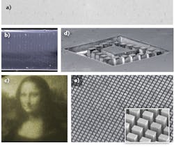
Selectively etched structures
In addition to creating in-chip silicon devices, the team can create other 3D microstructures including microfluidic channels, through-silicon vias, and large-area micropillar arrays, and can even perform laser-slicing of silicon wafers by selectively removing the laser-modified parts of the wafer that have a disrupted crystal structure using an acid-based solution.
Inspired by the successes of "on-chip" devices on silicon and other materials, the team coined the term "in-chip" devices as a shorthand descriptor of the new technique. "We achieve this by exploiting feedback dynamics arising from nonlinear laser-material interactions, leading to controllable building blocks," says Onur Tokel of the Department of Physics at Bilkent and lead author of the paper (staff.bilkent.edu.tr/onurtokel).
"In any 3D fabrication method, there is a tradeoff between speed, resolution, and complexity. With our approach, we are hitting the sweet spot," says Serim Ilday, a coauthor from the Department of Physics at Bilkent.
Ömer Ilday, another co-author of the paper and member of the Electrical and Electronics Engineering and Physics Departments at Bilkent, adds, "It is likely that the method will enable entirely new in-chip devices, such as Si-photonics components that can be used for near- and mid-IR photonics, or meandering microfluidic channels that may be used to efficiently cool electronic chips."
REFERENCE
1. O. Tokel et al., Nat. Photonics, 11, 10, 639-645 (Oct. 2017); http://dx.doi.org/10.1038/s41566-017-0004-4.
About the Author

Gail Overton
Senior Editor (2004-2020)
Gail has more than 30 years of engineering, marketing, product management, and editorial experience in the photonics and optical communications industry. Before joining the staff at Laser Focus World in 2004, she held many product management and product marketing roles in the fiber-optics industry, most notably at Hughes (El Segundo, CA), GTE Labs (Waltham, MA), Corning (Corning, NY), Photon Kinetics (Beaverton, OR), and Newport Corporation (Irvine, CA). During her marketing career, Gail published articles in WDM Solutions and Sensors magazine and traveled internationally to conduct product and sales training. Gail received her BS degree in physics, with an emphasis in optics, from San Diego State University in San Diego, CA in May 1986.