MATERIALS PROCESSING: 'Femtoprint' targets low-cost fabrication of in-glass microstructures
A three-year European Union (EU) project called Femtoprint, backed by the "Nanosciences, nanotechnologies, materials and new production technologies" theme of the EU Seventh Framework Programme (FP7), was inaugurated in May 2010 with $3.2 million dollars (€$2.5 million).1 The goal of the project is to accelerate the volume fabrication of in-glass microsystems that integrate optical, fluidic, and mechanical functions such as lab-on-a-chip devices or force and displacement sensors. Because such devices typically need to be manufactured in multiple steps with costly infrastructures and high capital investments such as cleanrooms, cost is prohibitive for small- and medium-volume fabrication facilities.
Reducing cost
Coordinated by the Eindhoven University of Technology (TUE; Eindhoven, the Netherlands), the Femtoprint project will use femtosecond lasers to create 3D patterns in glass without producing any particles and without requiring contact with the air, thus eliminating the need for a costly cleanroom environment. Unlike traditional laser-manufacturing processes, the Femtoprint process uses a very low-average-power laser (not more than 220 mW–about the power of a bright LED) to tailor and modify the glass matrix so that it behaves differently from the unmodified bulk glass.
Incredibly, Femtoprint creates these patterns using a one-step process–very different from traditional layer-by-layer techniques–in a compact housing that is eventually envisioned to operate much like a desktop printer, taking in sheets of glass and turning out microsystems with a combination of laser processing and etch steps.
The principle is to use tightly focused low-energy femtosecond pulses–below the ablation threshold–to tailor the glass matrix structure. Localized densification effects are observed, leading to a locally enhanced etching rate and increased refractive index. After exposure, the regions exposed to the laser-beam can be selectively etched, used as waveguides, or can form self-organized patterns as demonstrated by P. Kazansky, a Femtoprint partner.2, 3 At low pulse energies, the laser-affected zones are believed to be locally densified, although some aspects of the laser-matter interaction remain elusive.
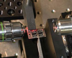
The combinations of waveguides with other microstructures have been demonstrated and create new opportunities for system integration at the microscale as illustrated by a displacement sensor (see figure). The Femtoprint project will build on this preliminary work to industrialize the process and to expand its applicability to a large number of users.
Reducing the footprint
An important component of the project is to reduce cost not only by the very one-step and cleanroom-free nature of the Femtoprint process but by reducing the size of the femtosecond laser to something on the order of a shoebox. This task is the responsibility of Amplitude Systemes (Pessac, France), while Eindhoven University of Technology together with its European partners (University of Southampton, CSEM, EPFL, Mecartex, Quintenz, and AlphaNOV) is primarily responsible for refining the effects of laser light on fused silica as well as for implementing the printer's components such beam-shaping and specimen-positioning devices.
"We think that offering the possibility to a large pool of users, such as small companies, to produce their own microsystems using a three-dimensional process will not only offer new technological horizons but will also boost innovations in microsystems by providing a means for rapid prototyping," says Yves Bellouard, TUE assistant professor and Femtoprint scientific coordinator.
REFERENCES
1. Project web site at www.femtoprint.eu.
2. A. Marcinkevičius et al., Opt. Lett., 26, 277-279 (2001).
3. Y. Shimotsuma et al., Phys. Rev. Lett., 91, 247405 (2003).
4. Y. Bellouard et al., Opt. Exp., 13, 6635-6644 (2005).
About the Author

Gail Overton
Senior Editor (2004-2020)
Gail has more than 30 years of engineering, marketing, product management, and editorial experience in the photonics and optical communications industry. Before joining the staff at Laser Focus World in 2004, she held many product management and product marketing roles in the fiber-optics industry, most notably at Hughes (El Segundo, CA), GTE Labs (Waltham, MA), Corning (Corning, NY), Photon Kinetics (Beaverton, OR), and Newport Corporation (Irvine, CA). During her marketing career, Gail published articles in WDM Solutions and Sensors magazine and traveled internationally to conduct product and sales training. Gail received her BS degree in physics, with an emphasis in optics, from San Diego State University in San Diego, CA in May 1986.