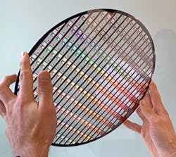
Starting from a revision of the classical optical laws of reflection and refraction, Harvard’s Federico Capasso imagined metasurfaces and metalenses and how these devices could be used to create nanosized flat lenses with the potential to revolutionize multiple optical applications.
Now, the first metalens applications are a reality and the entire value chain for high-volume production is coming to fruition. This flat lens technology is revolutionizing the optics used for sensing and imaging. There are challenges, as well, to overcome before metalens technology can fulfil its potential.
The development of metalens technology
Photonic devices have several advantages over traditional electronics in terms of miniaturization and speed of data transmission. But until recently, the size of lenses has been constrained by the material properties (refractive index and dispersion) of glass or, in recent decades, plastics. As a result, current optical technology is still largely based on a relatively medieval tool, the glass lens, which researchers haven’t been able to improve beyond achieving greater precision in shaping and grinding. Until more recently, there was no way to significantly shrink the size of lenses used within cameras, microscopes, telescopes, and other optical equipment.
In 2016, researchers at Harvard University’s John A. Paulsen School of Engineering and Applied Sciences (SEAS) demonstrated the first metalens that worked efficiently within the range of visible light, covering the entire spectrum of colors from red to blue. Calling the waveguides “nanofins,” the SEAS team led by Capasso designed their metalens to focus light onto a single point approximately 400 nm across. In contrast to traditional lenses, Capasso’s team used a single thin, flat structure with multiple waveguides—like tiny pillars—arranged in specific patterns made from titanium dioxide (TiO2) approximately 600 nm long.
Their metalens was the first to focus the entire spectrum of visible light and offered optical performance better than any current commercial lenses. Specifically, because metalenses are flat (planar) and ultrathin, they do not produce chromatic aberrations. They are also achromatic, because all wavelengths of light pass through virtually simultaneously.
Metalenses have the added advantage of tunable dispersion (i.e., the ability to manipulate how colors of light are dispersed), as opposed to glass or other traditional materials that have fixed dispersions. But perhaps most importantly, metalenses can be mass-produced in existing CMOS semiconductor foundries, which enables massively parallel wafer-scale integration of optical systems.
During the last six years, metalens research has continued unabated. Examples include research by Tunoptix, an optics startup cofounded by the University of Washington to develop metalenses for imaging in satellites at the Washington Nanofabrication Facility.
Similarly, in the quest for miniaturization, scientists at the Center for Integrated Nanostructure Physics (South Korea), in collaboration with researchers from the University of Birmingham, worked on credit-card-thick flat lenses with tunable features. These optical devices, made of graphene and a punctured gold surface, could become optical components for advanced applications, such as amplitude tunable lenses, lasers (i.e., vortex phase plates), and dynamic holography.1
Other researchers focused on the principles of metalens design and different types of novel metalenses—including label-free sub-resolution, nonlinear, artificial intelligence-aided, multifunctional, and reconfigurable—as well as how to remove focusing aberrations, the essential condition to realizing metalens objectives and microscopy.2
Researchers found a solution for reducing the size of cameras by combining both metalenses and ‘spaceplates,’ an optic that effectively propagates light for a distance that can be considerably longer than the plate thickness. Such an optic would shrink future imaging systems, opening the possibility for ultrathin, lens-free cameras and a bigger sensor.
Current metalens applications
A pioneer in commercializing metaopticsis Metalenz, a Boston-based fabless semiconductor optics company spun out of Capasso’s lab at Harvard University in 2016. As shown in Figures 1, 2, and 3, the company’s first generation of products, dot pattern projectors and imaging components for 3D sensing, greatly simplify the footprint and complexity of existing modules. Furthermore, as a completely planar optical element, Metalenz technology paves the way for optics and semiconductor manufacturing to take place within the same foundry. The company’s second generation of products will enable full polarization sensing at a mobile form factor, unlocking everything from spoof-proof facial authentication for notebooks and Android devices to autonomous machine vision.
The demonstration successfully confirmed that, in the future, only half or even fewer optical components will be needed to support bright, 3D scene illumination of smartphone cameras. These advantages, combined with a reduction in space between components means smartphone manufacturers can get a technical competitive advantage. As Berthold Schmidt, CEO of TRUMPF Photonic Components notes, with the development of polarized VCSELs, they can address demanding 3D illumination applications not only in smartphones but also in organic light-emitting diode (OLED) screens and in virtual- and augmented-reality (VR and AR) applications. Market release of their next-generation advanced polarized VCSEL is planned for 2023.
II‐VI Inc., a wafer-level diffractive optics provider, developed a combined VCSEL and high-efficiency multifunctional metalens system based on a proprietary platform to enable ultracompact optical sensors for a broad set of applications, such as consumer electronics, automotive, life sciences, and industrial markets. These new metalenses achieve multiple optical functions with extremely high efficiency on a single surface for a broad range of wavelengths. In one implementation, this metalens both collimates and splits the light from VCSELs into a highly uniform grid of thousands of infrared beams projected onto the scene. Optical sensors reference these grids to accurately construct the scene in 3D; the combined metalens and VCSEL systems enable differentiated ultracompact 3D-sensing cameras for consumer electronics and automotive applications.
Another pioneering metalens company is NIL Technology (NILT), a Danish optical solutions company, which has been developing solutions in replication and nanoimprinting using advanced and complex nanostructures for nearly two decades. NILT is now able to combine meta and diffractive optics to build thinner, flatter, lighter solutions compared to those possible with refractive lenses. As a result, optical applications can be significantly reduced in size and complexity. And by combining technologies, the imaging quality and functionality of optical applications can be increased.
NILT's meta-optical elements (MOEs) were demonstrated in 2021, with a record-high absolute efficiency of 94%. Today, they are working with major OEMs to develop numerous meta-optical solutions in 3D sensing, consumer electronics, and AR/VR/mixed reality (MR).
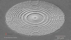
Heidelberg Instruments/Multiphoton Optics developed a ground-breaking approach for metalens fabrication with a two-photon polymerization (TPP) technology based on Multiphoton Optics’ MPO 100 direct laser-writing system. This system offers additive generation of meta-atoms with a diameter down to 100 nm in a single process step. As a result of its nonlinear absorption, TPP provides feature sizes below the diffraction limit and enables varying diameter and height of the meta-atoms, offering an additional freedom in design for polymer-based metalenses. Furthermore, the use of optical polymers means the applications can be used as functional structure or master for replication technologies. A TPP-fabricated metalens with a focal length of 100 µm at 630-nm operation wavelength is shown in Figure 4.Future challenges
Cost is a major challenge for metalens fabrication because the difficulty aligning nanoscale elements precisely on a centimeter-scale chip is expensive. There are also technical challenges—metalenses do not transmit light as efficiently as traditional lenses, which is an important drawback for applications such as full-color imaging. Metalenses are also too small to capture a large quantity of light, which means, at least for now, they are not suitable for producing high-quality photographs.
For metalenses to come to full fruition, a new supply-chain and ecosystem will be needed to bring together manufacturers, material suppliers, design houses, and integrators to provide a clearer understanding of how to turn the potential of metalenses into tangible improvements for end-customers, according to Lieven Penninck, founder of PlanOpSim, a Belgian startup developing numerical modeling software for metalenses.
For this reason, PlanOpSim developed an integrated software system covering the design process of a metasurface—from the nanosized metaatom through components of millions of metaatoms and connecting to widespread ray-tracing tools for system optimization. Their multiscale simulation approach treats the subwavelength structures of the metaatoms with a full Maxwell solution and applies appropriate approximations on the component and system scale where a full wave solution is extremely time and memory consuming.
Another company providing software tools for different stages of metalens design is Ansys Lumerical. Each unit cell of the metalens can be simulated via the company’s FDTD or RCWA to determine ideal design parameters, such as layer thicknesses, and to create a library of cells for different phase, transmission, and polarization responses. Using the recently acquired Zemax OpticStudio, the target phase profile of a lens within a complex system can be optimized for a given application, which allows a user to design a metalens from the available unit cells to achieve the desired phase response, and even save the layout to global distribution service (GDS). The full lens can be simulated with Lumerical FDTD to verify it works as designed and to understand any undesired scattering that may occur. Finally, the full electromagnetic field after propagation through the lens can be imported from FDTD into OpticStudio for subsequent optimization.
Despite some remaining challenges, the progress made to date with metalens technology shows it holds great promise for the continuing development of optical, imaging, and display systems. New metalenses can be made within the same fabrication plants as computer chips, and with mass production comes the potential to scale up at a much lower unit cost. These advantages, together with superior performance, reduced size and weight, and increased functionality and efficiency over traditional lenses, make metalenses a potential game-changer for the optical industry, with the opportunity to revolutionize the way we see the world.
REFERENCES
1. See https://bit.ly/38HY502.
2. See https://bit.ly/3KAJSiW.
3. See https://bit.ly/3vzC0ty.
About the Author

Antonio Raspa
Ultrafast Solid-State Laser Product Manager, Luxinar
Antonio Raspa is ultrafast solid-state laser product manager at Luxinar (Kingston upon Hull, U.K.), and an editorial advisory board member at Laser Focus World. He has more than 35 years of experience with solid-state laser design, photonics components, and fiber optics.
He holds a MSc degree in Electrical Engineering from Politecnico di Milano with a specialization in Quantum Electronics. Before joining Luxinar, he served as senior photonics program manager at the European Photonics Industry Consortium (EPIC; May 2020 – September 2022), preceded by Quanta System (1988-2000) as R&D manager for the development of solid-state laser sources and custom photonics systems for industrial and scientific applications. During this period, he participated, as Ozone LiDAR specialist, to the Italian research program in Antarctica. He then worked at Trumpf (2000-2008) and Rofin-Sinar (2008-2009) as a Product Manager for industrial laser products and processes. In 2009 he returned to Quanta System, organizing and managing a new plant for the production of sterile optical fibers for surgery.


