The concept of metamaterials emerged at the turn of the century. By the mid-2000s, labs around the world were making headlines by demonstrating science-fictional invisibility cloaks. Yet fabricating 3D metamaterials for optical wavelengths remains difficult because of the small scale required.
About a decade ago, Federico Capasso at Harvard University (Cambridge, MA) wanted something more practical for optics. The success of flat 2D electronic integrated circuits inspired him to explore prospects for 2D optical metasurfaces. That led to the discovery that high-contrast subwavelength dielectric structures can bend light sharply enough to produce ultrathin optics, which led to metalenses—individual flat optical devices that focus light.
Today, metalenses have demonstrated promise in outperforming conventional solid refractive lenses for some applications. Metalenz (Boston, MA), a startup spun out of Capasso’s lab, is producing metalenses for specialized smartphone sensors.
“We can produce brighter and more uniform images from metalenses than from conventional smartphone cameras because our camera is flat,” says company CEO Rob Devlin. He noted that replacing conventional refractive optical cameras now used in smartphones with metalens cameras can eliminate camera bumps and holes in their displays. And more applications are coming.
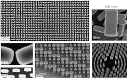
A close look at a metasurface
A metalens is made by depositing an array of subwavelength “pillars” of a high-index material on a flat substrate on the order of a millimeter thick, with both materials transparent at the transmitted wavelength. The pillars, which Capasso calls “meta-atoms,” are individual subwavelength building blocks that form the metasurface. Their shapes, separation, and placement on the substrate are tailored to make the metalens bend transmitted light in the desired way. Typical metalenses are one to a few millimeters across, but they can be made wider.
Figure 1 shows scanning electron microscope images of subwavelength pillars in a few simple metalenses, made by depositing atomic layers of titanium dioxide (TiO2), which is transparent in the visible, on a millimeter-thick substrate. The walls are vertical and smooth. Use of high-index materials such as TiO2 produces strong interactions between the incident light and the metasurface, according to Devlin. “If the index is too low,” he says, “a lot of light can pass through the device without interacting with the pillars.” This reduces focusing efficiency.
The pillars must be transparent and have a high refractive index at the operating wavelength. Titanium dioxide pillars are used in the visible range, where the refractive index ranges between 2.4 in the red to 2.8 in the blue. Silicon is used in the near-infrared (near-IR), where it is largely transparent and has a refractive index of 3.4.
“For scaling to mass production, you can’t pick a better material than silicon,” Devlin says, because it is so widely used in electronics and is very well understood. However, silicon absorbs strongly at visible wavelengths and is not completely transparent in other bands. Silicon nitride (SiN) is more transparent in the visible, and silicon-rich SiN can be made with a refractive index of 2.74 at 685 nm. However, SiN suffers from high absorption in certain visible bands, limiting its potential for broadband metalenses.
Interest is high in visible and near-IR wavelengths because of their wide use in imaging, communications, and other applications, but other materials are needed for other bands. According to Tian Gu of the Massachusetts Institute of Technology (MIT; Cambridge, MA), chalcogenide glasses are used in the mid- to long-wavelength infrared (IR). For example, lead telluride is transparent at 5.2 µm, and can be deposited on a calcium fluoride substrate in 650-nm layers, which are only one-eighth of the free-space wavelength, a smaller fraction than for the materials used in the visible or near-IR metalenses. The pitch between pillars in this mid-IR metalens was 2.5 µm, half of the free-space wavelength. Longer wavelengths simplify some aspects of mid-IR metalens fabrication because the individual pillars need not be as small as in the visible, but the materials needed are not as well developed as silicon.
The short end of the visible spectrum and the near ultraviolet pose more problems, as the features are much smaller and materials and processes are less developed for large-scale metasurfaces. Gallium nitride (GaN) and SiN are potential options.
The behavior of a metasurface is mostly controlled by the structure of the meta-atoms, in contrast to traditional bulk optics that rely on the optical component’s geometry, Gu says. When the light enters the metalens, each pillar or meta-atom will delay and scatter the light differently, re-emitting the light as a separate wavefront. Then, the arrangement of the pillars will delay the wavefronts, stitching them together to produce the new wavefront that emerges from the metalens. The process in theory diffracts some 95% of the light through the metasurface, according to Gu, and gives meta-optics advantages in size, weight, performance, transmission efficiency, and cost over conventional refractive lenses.
The pillars can be fabricated in many shapes and forms as long as they remain smaller than the operating wavelength. Some pillars are rectangular slabs or cylinders, while others are more complex. Their size and orientation can vary across the surface of a metalens (see Fig. 1). Metasurfaces have been demonstrated that can produce arbitrary reflection and refraction, that can focus light and/or control polarization, to project holographic images, and so forth.
Electromagnetic theory describes both metamaterials and metasurfaces, and early work included metallic components as well as dielectrics in both 2D and 3D materials. However, theoretical analysis showed that all-dielectric metasurfaces with high contrast scattered light more effectively than if they include metal layers. Today, all-dielectric structures prevail for metasurfaces.
Each pillar acts as a resonator or a vertical waveguide, which can be tuned across a range of 2π in phase in TE and TM modes; this is longer than the maximum possible for thin metal rods. Customization and arrangement of the subwavelength pillars allows metalenses to diffract and bend light with finer precision than is possible with bulk refractive optics. The ability of subwavelength structures within metalenses to direct light is similar to the ability of small metal radio antennas to direct radio waves that are much larger than the antennas.
Advantages of metalenses
A key advantage of metalenses over solid refractive lenses is that the flat optics project flat images onto flat surfaces, but refractive optics have curved surfaces that project curved images onto curved surfaces. That’s a problem for cameras because they usually need to project onto flat surfaces such as sensors and screens. One refractive lens could project an unaberrated image onto a curved surface, but three or four solid lenses are needed to remove the aberration when the lens is projecting onto a flat screen. A single metalens could do the job.
That’s important for smartphone cameras. The tiny plastic lenses in today’s smartphone cameras can do wonders, but their stack of three or four lenses is 6 mm high, which produces a bump on a smartphone that is a stylishly thin 5 mm. Addition of other sensors that require focusing optics without full color poses a similar problem—a hole must be cut in the screen to accommodate the full depth of conventional refractive focusing optics.
Diffractive or holographic lenses are flat and can project flat images and share some other advantages of metalenses, but they have their own limitations. Metalenses can manipulate the polarization of light; diffractive lenses cannot. High numerical aperture and selection of polarization have been demonstrated in metalenses, but not in diffractive lenses. Metalenses also can be made tunable in various ways. MIT engineers recently fabricated a metalens from a novel phase-change material in which a change in temperature rearranges its atomic structure and thus shifts how it interacts with light without moving it mechanically.
In addition to outperforming diffractive lenses in some areas, one study concludes, metalenses have more degrees of freedom because they have a potentially unlimited range of nanostructures. However, the theoretical descriptions of metalenses require complex mathematics, so new tools must be developed that can design the nanostructures needed to manipulate the light.
Fabrication advantages
A crucial attraction of metalenses is the potential of adapting the photolithographic processes developed for semiconductor production to mass-produce the nanostructures.
Laboratory production has depended largely on electron-beam (e-beam) lithography. E-beam fabrication is good in the laboratory because it has flexibility, extremely fine control, and high resolution. Although, it writes one thing at a time, so it can be tedious. Deep-ultraviolet (deep-UV) lithography can be used for testing, but the technology is better suited for producing multiple copies of chips than for testing single copies of new designs.
Metalenz is now using deep-UV lithography on 30-cm wafers in foundries that also make semiconductor electronics.
“We can use deep-UV lithography to produce about 5000 lens dies measuring 3 × 3 mm or 12,000 2 × 2 mm dies on a single wafer at up to 100 wafers per hour,” Devlin says. They use glass wafers that are 775 µm thick, the same thickness the foundries use to make silicon electronics.
Figure 2 shows a 30 cm wafer with 5000 TiO2 metalenses of various sizes on its surface. Each small rectangle visible on the surface contains the same pattern of metalenses in several sizes. At center is a 1 mm lens, with the magnification at right showing pillars on the surface.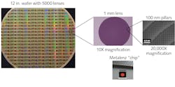
The company’s first-generation products are fairly simple designs for face recognition systems based on structured light built into smartphones for security. VCSELs built into the phone flash at 850 nm or 940 nm to provide the structured light. Metalenses typically 1 to 3 mm in diameter collect the returned light and focus it onto a flat sensor. Devlin calls it “a good entry market,” as they have already demonstrated the technology and it is available for use. The near-IR security application does not require wide spectral range, allowing the use of first-generation metalenses with the relatively simple array of cylindrical pillars shown at the right of Figure 2 to focus the narrow-band light onto the planar sensor. Multiple refractive lenses would be required to focus the collected light evenly across a planar surface, making them hard to fit into a thin smartphone.
Lidar is another popular sensing application for smartphones, which Apple introduced in its iPhone 12 line. Similar to face recognition, lidar does not require a broad range of wavelengths, so it can use metalenses to focus returned light onto flat sensors. Existing smartphone lidars can measure distances to 5 m, but the technology could be extended to longer distances for mapping in augmented reality. Three-dimensional profiling is another potential application, but would require further development.
A further step is full-color imaging. The simple metalens shown in Figure 2 does not focus all wavelengths to the same distance, so it is not achromatic enough for color cameras. That requires using a more diverse range of pillar shapes and sizes to focus all colors in the image to the same plane—that will come in a future generation camera. Once such lenses are available, they could also replace the imaging cameras in smartphones, removing the “bump” in current versions and removing the camera hole in the screen.
Other fabrication techniques
Techniques other than photolithography also are being investigated for metalens fabrication. One is depositing a pattern on one substrate, then transferring it to another substrate, similar to the flip-chip technique used in integrated photonics to fabricate III-V light emitters on one substrate, then remove them for bonding onto silicon integrated electronics. An option being investigated for IR metasurfaces is direct laser writing, in which a high-power laser beam ablates material from the surface or changes other properties of the surface. Chemical self-assembly of fabricating nanospheres that align to each other is being investigated as well. Other options for reproducible large-scale production include roll-to-roll nanoimprinting and soft lithography using elastomers rather than harder inorganic semiconductors.
It remains an open question how well the silicon foundry technology being developed for integrated photonics (see “Advanced 3D printing makes light work of mini optical communications device fabrication”) will work with metalenses and other metasurfaces. The current generation of integrated photonics transports light horizontally through waveguides or optical fibers, and those foundries are optimized for large-scale production of such devices. Metasurfaces direct light through free space, at least for short distances, so they may require foundries optimized for such devices.
Outlook
The past decade of research has brought impressive progress in metasurfaces in general and metalenses in particular. An impressive volume of research shows that metalenses are looking good for the first practical optical application of metamaterials. Groups at the California Institute of Technology (Pasadena, CA), Columbia University (New York, NY), the University of Michigan (Ann Arbor, MI), the University of Rochester (Rochester, NY), and the King Abdulla University of Science and Technology (Saudi Arabia) have active programs.
Metalenz, recently emerged from stealth mode, is only one of the promising startups. Tunoptics, a spinoff from the University of Washington (Seattle, WA), has funding from DARPA to develop metalenses for satellite imaging. Lumotive (also in Seattle) is developing liquid crystal metasurface technology for high-resolution beam-steering lidar. More companies are likely to follow if the metalens technology lives up to its promise to flatten optics and further miniaturize optical devices.
About the Author

Jeff Hecht
Contributing Editor
Jeff Hecht is a regular contributing editor to Laser Focus World and has been covering the laser industry for 35 years. A prolific book author, Jeff's published works include “Understanding Fiber Optics,” “Understanding Lasers,” “The Laser Guidebook,” and “Beam Weapons: The Next Arms Race.” He also has written books on the histories of lasers and fiber optics, including “City of Light: The Story of Fiber Optics,” and “Beam: The Race to Make the Laser.” Find out more at jeffhecht.com.