Grayscale lithography system enables high-volume production of freeform micro-optics
Making lenses has evolved from a rare craft creating unique pieces 150 years ago to an industrial process where massive volumes of product with similar properties are produced in batches. Since then, lenses have left the spherical world behind and become freeform, and sizes shrank down to millimeter and even sub-micron scales. Major developments have led to further down-scaling and smart-optics, where interactive functionality is added through close integration with other elements.
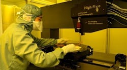
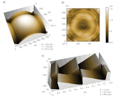
Grayscale lithography is a mature technology that enables mass production of micro-optical, microfluidic, or micromechanical components and integrated structures (see Fig. 1). Application areas of such components include special lighting systems for the automotive market, lightweight sensor systems for space missions, lab-on-a-chip systems for protein analysis, and miniaturized integrated optical systems such as AR/VR goggles (see Fig. 2).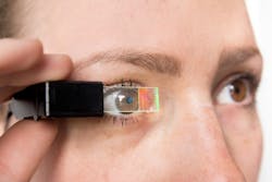
Why grayscale stepper lithography?
Various photolithographic methods for making micron-level structures have evolved to address different precision, flexibility, and cost requirements. Because laser beam lithography uses a laser beam to directly address an arbitrary point on the surface, it provides a very high degree of flexibility. However, the flexibility provided by scanning comes at the expense of limited throughput and elevated costs.
Another process, electron-beam lithography, is used for producing photomasks or reticles when precision and zero-error rates are more important than throughput. Such masks are used in mask aligners that transfer imprinted patterns onto the whole wafer in one step. This is a highly productive technology used where larger error budgets are accepted. The stepper lithography is a balanced compromise between flexibility and throughput.
But, what about grayscale? Classical lithography works primarily with binary structures—that is, the structure height is defined by the height of the coated photosensitive resist and does not vary across the whole wafer. Grayscale lithography allows for tailoring of z-dimension through exposure with intensity-modulated light. The gradual intensity distribution in the projected pattern causes a gradual change in the resist, which leads to a locally different chemical solubility in alkaline media. When developing the substrate, a surface profile forms in accordance with the deposited dosage variation.
Experts at the Fraunhofer Institute for Applied Optics and Precision (Fraunhofer IOF; Jena, Germany) collected decades of experience with various lithographic procedures. Multiple experiments resulted in a combination of the digital reticle, a stepper, and grayscale technology. While the grayscale lithography system from Fraunhofer IOF illuminates areas similar to the classical approach, the projected pattern stems from a spatial light modulator, a tiny grayscale projection display.
Because it’s smaller than the mask in a photolithographic system, it needs a sophisticated stepper and stitching technology to process larger areas. Nevertheless, the approach has significantly greater throughput capabilities compared to ultra-precision diamond turning or two-photon polymerization.
Compared to conventional photolithography, grayscale lithography has two eminent advantages. First, it is flexible and can change the pattern for each illumination step, and second, it allows for gradients in the illumination pattern. As a result, an arbitrary topography in a photoresist can be created.
How does it work?
The HighFive C high-dynamic grayscale lithography system, which was established in recent years, uses various wavelength UV LEDs as a 2 W optical power light source. Sophisticated optics adapt the illumination profile of the LED to the rectangular shape of the subsequent micro-display, which in turn generates the required projected pattern.
Thanks to the working principle, every pixel can modulate the UV polarization angle with 10-bit resolution, which defines an amount of the available light levels within the projected image. After extracting the necessary polarization state with a beamsplitter, the final image is projected onto the substrate via an exchangeable objective. Having a choice between 1.25x down to 100x demagnification, users can tailor processing time and resolution tradeoffs for their application. More details of the exposure concept have been published elsewhere.1
The resist-coated substrate is placed on a high-speed motion positioning system with a travel range of 500 × 500 mm2. Numerous feedback systems such as linear encoders, an optical autofocus, laser interferometers, and a temperature control unit allow for a repeatability better than 100 nm. The accurate orientation of lithographic patterning with respect to a previous generated structure level is assisted by an additional alignment microscope. Figure 3 shows a schematic of the grayscale lithography setup.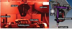
Applications
Grayscale photolithography has been used for the efficient production of a variety of different refractive and diffractive optical structures (see Fig. 4). Being challenging for other manufacturing approaches, the generation of high-fidelity arbitrary shapes is a task, where the HighFive steppers excel. Among those are customized micro-lens and -prism arrangements, which serve as building blocks for deterministic diffusers, the beam-shaping elements. Compared to holographic types, they allow for a spatially resolved variation of light’s angular distribution function to create defined far-field patterns.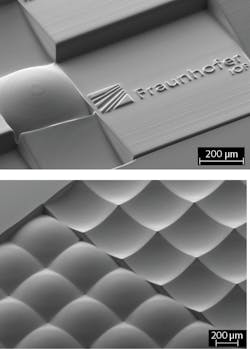
Creating large-scale micro-optics masters
For mass production, a positive master structure is molded into a negative polydimethylsiloxane (PDMS) stamp, which is used for replication of fully populated wafer substrates carrying hundreds of optical chips in one step (see Fig. 6). The micro-optics industry follows the semiconductor industry, reducing the manufacturing costs by increasing (master) substrate size and pushing the number of chips per wafer to the boundaries. The HighFive line steppers at Fraunhofer IOF are able to pattern up to 12 in. (300 mm) substrates and is prepared to address wafers up to 18 in. (450 mm).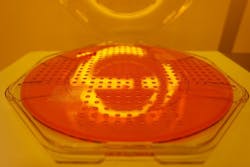
Future development potential
There are several major directions where the scientists are now focused, including increasing the resolution below 600 nm, processing highly curved substrates by introducing additional degrees of freedom, and reduction in process time by applying advanced writing strategies.
After all, based on years of research experience and in close collaboration with industry, the HighFive grayscale photolithography stepper has been brought to maturity and is ready for mastering advanced wafer-level optics. It is well suited (but not limited) to pattern deep and high-resolution surface profiles for a wide variety of microstructures with a high direction isotropy as a result of a refined working principle.
REFERENCE
1. H. C. Eckstein et al., Proc. SPIE, 9780, 97800T (Mar. 15, 2016); https://doi.org/10.1117/12.2219099.
About the Author
Andreas Thoss
Contributing Editor, Germany
Andreas Thoss is the Managing Director of THOSS Media (Berlin) and has many years of experience in photonics-related research, publishing, marketing, and public relations. He worked with John Wiley & Sons until 2010, when he founded THOSS Media. In 2012, he founded the scientific journal Advanced Optical Technologies. His university research focused on ultrashort and ultra-intense laser pulses, and he holds several patents.
Dmitriy Mitin
Postdoctoral Researcher, Department Microoptical Systems
Dr. Dmitriy Mitin is Postdoctoral Researcher in the Department Microoptical Systems at the Fraunhofer Institute for Applied Optics and Precision (Fraunhofer IOF; Jena, Germany).
Robert Leitel
Group Leader, Advanced Micro-optical Components
Dr. Robert Leitel is Group Leader for Advanced Micro-optical Components at the Fraunhofer Institute for Applied Optics and Precision (Fraunhofer IOF; Jena, Germany).