Old-timers know optical computing is not all new. Optical processing that generated military maps by Fourier transforms of synthetic-aperture radar data were so successful in the 1950s that they were classified, although electronic fast Fourier transforms eventually won out. In the 1980s, the late John Caulfield told me how a new generation of optical computing could do things we could never imagine, but couldn’t balance your checkbook; yet again, electronics proved faster, better, and cheaper. Now that semiconductor features have shrunk to the nanometer scale and Moore’s law is running out of room, a new generation of integrated photonics could boost the speed and processing power of artificial intelligence (AI) beyond what electronics can provide.
The quest for artificial intelligence
AI has its own long history of promises that have proved hard to fulfill. AI’s roots literarily came from science fiction. Isaac Asimov’s famed robot stories inspired Marvin Minsky, who as a young professor launched the MIT Artificial Intelligence Laboratory in the early 1960s. Like optical computing, AI was slow getting off the ground, and suffered an “AI Winter” in the 1980s and early 1990s.
Its revival came from machine learning, which programs computers to gather and analyze large volumes of information using neural networks, which like the human brain have massive interconnections among their processors. Machine-learning systems have found applications ranging from filtering spam from your email to recommending films on Netflix, but their most famous uses are beating humans at complex games such as Go and chess.
Deep learning extends on machine learning by using more-complex neural networks to tackle more-complex tasks, including speech recognition and autonomous driving. However, deep learning requires processing huge volumes of information using complex processes such as matrix vector manipulation, and electronic computers cannot keep up with the rapidly increasing demands. Developers are looking to silicon photonics to provide the needed boosts of speed and power.
An ‘alien’ intelligence
Although neural networks inspired the design of machine learning, AI does not work like the human mind. In machine learning, “the core computational algorithm is not fully provided by a programmer, but automatically generated or improved by a computer system through experience,” wrote Qixiang Cheng, now at the University of Cambridge (Cambridge, England), in a review article.1 A machine-learning system learns by processing input information using special algorithms designed to recognize patterns in the data. Images often are a starting point, but the systems analyze other types of data as well.
You might think of an AI as an alien mind, and it has different skills than humans. An AI performs brilliantly at games with well-defined rules that it has played many times; it can beat human champions, whom we consider highly intelligent. Yet AIs must be trained for specific tasks, and can’t recognize other things not in the training set. An AI chess champion couldn’t drive a car around the block, and a self-driving car AI would not know what to do about a large red truck with hoses attached and light flashing that is stopped in the road unless it had previously learned about a fire truck doing all those things. Humans are more adaptable.
Deep learning expands on machine learning by sorting through larger data sets using neural networks with multiple levels of processing. For example, a neural network may use multiple factors to recognize a face, such as nose shape, hair color and pattern, eye color, skin color, space between the eyes, and positions of other facial features. Mathematical processing of many levels of data using tools including matrix-vector multiplication, convolution, and Fourier processing has brought success in applications including speech recognition, image classification, and driving autonomous vehicles.
Success requires processing large volumes of data very quickly. Driving is a particular challenge because it must be done in real time; a self-driving car cannot stop in the middle of the road and wait to identify the unknown thing moving across the road. That makes latency a problem when handling large volumes of data. Modern electronic computing is encountering practical limits not only in processing speed but in power consumption, which increases rapidly at high speeds and has forced designers to divide semiconductor processors into multiple cores for operation at more than a few gigahertz.
Developers hope that the combination of optical parallelism, photonic integration, and silicon photonics can bring latency down to meet the demanding limits of deep learning in applications like autonomous vehicles.
Integrated silicon photonics for AI
The most complex and time-consuming operations in deep learning are matrix-vector multiplications, in which an M-by-N matrix is multiplied by an N-dimensional vector (X). The input data is supplied electronically, then converted into optical form so the multiplication can be performed in the photonic integrated circuit, which yields the product an M-dimensional vector in the form Y = K ∙ X , which is returned to the electronics. That output may require further processing for use in the system.
Matrix multiplication requires multiple operations, which the natural parallelism of optics can perform simultaneously, and integrated photonics are far more efficient than older bulk optical technologies. Optical transceivers consume less power than electronic ones, and if an optical neural network can be trained completely, the matrix can be left passive for further operation without consuming further power. Optical matrix multiplication can be performed at rates up to the photon detection rate, typically around 100 GHz—much faster than electronic clock rates of a few gigahertz.
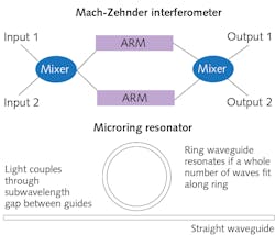
The two most common components in AI integrated photonic chips are Mach-Zehnder interferometers (MZIs) and microring resonators (MRRs), both shown in Figure 1. MZIs date back over a century. Two inputs at left mix, then are passed through two parallel arms where light is modulated to control its division between the two outputs at right. MRRs are more-recent inventions—tiny waveguide rings that can couple light through subwavelength gaps into other optical waveguides. Resonances occur along the lengths of the rings at wavelengths where a whole number of waves fits exactly around the length of the ring. Combining those two optical building blocks can make modulators, filters, multiplexers, switches, and computing elements.
Multiring resonators and MZIs can be combined with field-programmable gate arrays to perform optical vector matrix multiplication. Photonic deep-learning systems will use results of the operations to learn and recognize objects, and are expected to offer higher processing capacity and speed than purely electronic systems can now provide.
From research into development
Developers are benefitting from big investments over the past several years in research, development, and manufacturing of integrated photonics. That has fertilized the soil for a wave of integrated-photonics startups aiming at the AI market.
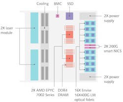
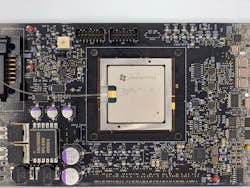
In March 2021, a Massachusetts Institute of Technology (MIT; Cambridge, MA) spinoff called Lightmatter (Boston, MA) introduced what the company calls “the world’s first general-purpose photonic artificial intelligence accelerator.” Named Envise, it’s a photonic module that can be plugged into leading models of AIs and neural networks to supercharge their performance, which in the AI world is measured in “inferences” per second. Envise includes an array of 16 Lightmatter photonic chips, and is built into a 4-U server blade format. It has 1 TB of DRAM, 3 TB of solid-state memory, and handles optical interconnections up to 6.4 Tbit/s. As shown in the schematic in Figure 2, the Envise also includes two lasers driving the photonic processors. The basic building blocks are arrays of identical MZIs assembled for matrix multiplication.Several other startups appear to have similar plans for speeding up AI processing for various applications with integrated photonics, but so far their public sites give little detail. Luminous.co (Mountain View, CA) has attracted funding from Bill Gates, and says it is focusing on concepts developed by CTO Mitchell Nahmias while he was studying at Princeton University.2 Nahmias’s earlier work focused on neuromorphic photonics, which uses integrated photonics to implement analog photonic operations.3
LightIntelligence (Boston, MA) is a startup focusing on optical neural networks, which jointed the MIT Startup Exchange in 2019. Its CEO and founder Yichen Shen graduated from MIT and was lead author of a Nature paper on deep learning with coherent nanophotonic circuits.4 As of July 26, 2020, it was trying to build the “world’s largest integrated photonic circuit.”
LightOn (Paris, France) was founded in 2015 and says it has developed the first large-scale hybrid digital/analog computing platform for AI applications.5 The company operates a service that allows customers to use the company’s optical processing units through a dedicated online cloud infrastructure.
Fathom Radiant (Union City, CA) says it is developing an optical interconnection fabric that can achieve long-range bandwidth of petabits per second at watt-level power over distances to 100 m. The company claims Jeff Bezos among its investors.
Optalysys Ltd. (Wakefield, England) is somewhat different; a 2001 spinoff of Cambridge University, it refocused on big data in 2013 and has focused on chip-scale photonics and Fourier optics for image recognition. Optalysys implemented its first chip-level Fourier engine in 2020.
Frequency combs for massive parallelism
A new level of more-massive optical parallelism is emerging from the laboratory, based on wavelength-division multiplexing of the thousands or millions of narrow spectral lines generated by optical frequency combs. Initially used in spectroscopy and metrology, frequency combs earned Theodore Hänsch and John Hall the 2005 Nobel Prize in Physics. The January 7, 2021 issue of Nature included two demonstrations of how integrated photonics incorporating frequency combs could increase the speed and information handling capacity of optical neural networks. The two approaches differ in detail, but appear fundamentally compatible.
A team led by David J. Moss of the Swinburne University of Technology (Hawthorn, Victoria, Australia) demonstrated a frequency-comb system in a convolutional neural network of a type inspired by the visual cortex, which can analyze data in ways useful in computer vision, speech recognition, and medical diagnoses. The output of an integrated photonic frequency comb is simultaneously interleaved in dimensions of time, space, and wavelength to perform the desired matrix vector multiplication. Moss says the researchers’ test focused on speed, reaching 11 trillion matrix vector operations per second by directly performing ultrafast convolutions. They then used that output to process images of 250,000 pixels at speeds of 3.8 trillion processes per second for facial-image recognition. One ingenious trick was to use chromatic dispersion to produce different time delays for signals at different wavelengths and then combine them according to wavelength.6
The group acknowledged that the results could not match the 200 trillion operations per second of high-end electronic neural networks. However, “there are straightforward approaches toward increasing our performance both in scale and speed,” the researchers write in Nature. “This approach is scalable and trainable to much more complex networks for demanding applications such as autonomous vehicles and real-time video recognition.”
A frequency-comb alternative
A second group reporting in the same issue described what they called an integrated photonic hardware accelerator called a “tensor core” that could perform trillions of multiply-accumulate operations per second. The tensor core is the optical counterpart of an application-specific integrated circuit (ASIC). One of the key tricks to speeding operation was to perform operations in memory rather than moving the data to separate processors, a technique the group demonstrated in 2019 using a phase-change material for scalar matrix multiplication.7
As described in the new paper in the January 7, 2021 Nature, the group added chip-based frequency combs and extended the power of the technique to perform a convolution operation in a single optical time step, says Abu Sebastian, a staff member of IBM Zurich (Switzerland) and a leader of the group. That convolution is a mathematical operation performed on two functions that outputs a third function that shows how the change of one form is changed by the other. Neural networks can require billions of operations on a single image or other datum, so the researchers wanted to prove that their photonic chip could perform trillions of operations per second.8
Their experiment used matrices with up to 9 × 4 elements, with up to four input vectors per time step, into which they fed multiwavelength signals from their frequency-comb chip. Modulating their matrix at 14 GHz, they could process 2 trillion multiply-accumulate operations per second. The trick is to translate a convolution operation into several matrix vector multiplication operations, which they accomplish by performing them in parallel via wavelength-division multiplexing, something impossible in electronics.
“This is just the beginning,” says Sebastian. “We expect that, with reasonable scaling assumptions, we can achieve an unprecedented PetaMAC (thousand trillion [multiply-accumulate]) operations per square millimeter” on the chip. That density is a factor of a thousand higher than in state-of-the-art electronic AI processors.
“Both approaches are quite scalable,” says Moss. In principle, they can be combined by adding his group’s fast direct optical convolution to its phase-changing chip memory.
Outlook
In a commentary on the two frequency comb papers in the same issue of Nature, Huaqiang Wu and Qionghai Dai share their excitement at the potential of photonics to succeed electronics for the demanding task of AI computing. Yet they note that present optical processors are small, and that building a practical optical computer “will require intense interdisciplinary efforts” and cooperation across many disciplines.9
The integrated-photonics computer revolution will not be an easy one, but the new advances demonstrate important new capabilities much needed for further progress in AI. State-of-the-art electronic chips now have nominal feature sizes of 5 nm, the width of 10 silicon atoms; the closer that electronic features get to the atomic level, the more quantum-mechanical their behavior becomes, and the better photonic chips look.
REFERENCES
1. Q. Cheng et al., Proc. IEEE, 108, 8, 1261–1282 (Feb. 10, 2020); https://ieeexplore.ieee.org/document/8988228.
2. See http://tcrn.ch/30SW6Pd.
3. A. N. Tait et al., Sci. Rep., 7, 7430 (2017); https://doi.org/10.1038/s41598-017-07754-z.
4. Y. Shen et al., Nat. Photonics (Jun. 12, 2017); doi:10.1038:/nphoton.2017.93.
5. See http://bit.ly/LightOnRef.
6. X. Xu et al., Nature (Jan. 7, 2021); https://doi.org/10.1038/s41586-020-03063-0.
7. C. Ríos et al., Sci. Adv., 5, eaau5759 (Feb. 15, 2019).
8. J. Feldmann et al., Nature, https://doi.org/10.1038/s41586-020-03070-1.
9. H. Wu and Q. Dai, Nature, 589, 25–26 (Jan. 7, 2021).
About the Author
Jeff Hecht
Contributing Editor
Jeff Hecht is a regular contributing editor to Laser Focus World and has been covering the laser industry for 35 years. A prolific book author, Jeff's published works include “Understanding Fiber Optics,” “Understanding Lasers,” “The Laser Guidebook,” and “Beam Weapons: The Next Arms Race.” He also has written books on the histories of lasers and fiber optics, including “City of Light: The Story of Fiber Optics,” and “Beam: The Race to Make the Laser.” Find out more at jeffhecht.com.


