Metalens enables mini microscopic imaging prototype
Microscope imaging resolution and performance improvements typically require large and heavy refractive optical elements. However, when designing compact imaging devices for mobile widefield microscopy or other imaging applications, engineers seek the low-profile, lightweight, power-efficient, and flat system architectures found in today’s mobile devices.
Some researchers have minimized optical component requirements with lensless imaging, achieving thin imaging system designs by discarding the refractive lenses. Central to this approach is the concept that the light that diffracts from an object contains all the information about that object—even if that light is not detected within the image plane of a microscope. Unfortunately, the illumination sources and computational imaging techniques required for retrieving visual information from a diffraction pattern limit the suitability of such techniques in time- and power-constrained applications.
Metalenses offer a more energy-efficient solution for ultracompact and wide-field imaging. At least that’s the contention of Tao Li, professor of engineering and applied sciences at Nanjing University in China. In pursuit of a compact integrated microscope system, Li's team mounted a metalens on a CMOS image sensor to create a prototype of a coin-sized imaging device. Their metalens-integrated imaging device (MIID) exhibits an ultracompact architecture with a working imaging distance in the hundreds of micrometers. Using a simple image-stitching process, they can obtain wide-field microscope imaging with large field of view (FOV) and high resolution.
Flat metalens advantage
Less is more with integration, especially when designing a pocket-sized microscope. That’s why Li’s team directly integrated the metalenses onto the CMOS image sensor to show the major advantage of the flat metalens. The metalenses were composed of amorphous silicon (α-Si) nanoposts designed by the geometric Pancharatnam–Berry (PB) phase on a SiO2 substrate, where the Si material was used for potential compatibility to full CMOS-based devices. After careful characterization of the imaging qualities with respect to the resolution, signal-to-noise ratio (SNR), and FOV, the researchers demonstrate the capability of this MIID for spectral focal tuning due to the large dispersion, and overcome the limitation of lens-free shadow imaging that cannot resolve the depth-of-field (DOF) of the object.
To eliminate the blind areas in multiple-images-stitching, they used a polarization-multiplexed dual-phase (PMDP) design (with respect to two circular polarizations) to access two sets of lenses with complementary image areas. A full stitched wide-field image is completed only by switching the polarization without any mechanical movement. As a result, the researchers achieved high-resolution images (∼1.74 μm almost limited by image sensor pixel) with a millimeter-scale image area (expandable to whole centimeter-scale CMOS sensor), which was ultimately implemented in a ∼3-cm-size device prototype. This ultracompact microscope system promises more exciting applications of metalens in high resolution, large FOV, and tunable DOF imaging.
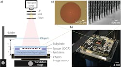
Metalens integration
MIID imaging setup schematics (see Fig. 1) show the optically clear adhesive (OCA) tape (69402) from Tesa (Norderstedt, Germany) that is used to transfer and fix the metalens on a DMM 27UJ003-ML USB 3.0 monochrome board camera from The Imaging Source (Charlotte, NC), which uses an ON Semiconductor (Phoenix, AZ) MT9J003 CMOS image sensor with 1.67 × 1.67 μm pixel size. The OCA is employed for its colorless transparency with high transmittance (>90%) in the visible and near-infrared ranges. The OCA tape, also used as the spacer medium of integration, provides a well-defined stationary thickness.
Once the metalens is mounted on the CMOS image sensor, the imaging distance is fixed, and a clear image can be acquired by tuning the object distance u (the distance between metalens and object) with the translation stage. Figure 1b shows the photograph of the highly compact MIID (here, v = 500 μm). It should be noted that, due to the complex medium layers in both image space and object space of the metalens, the parameters (u; v) here are effective ones containing the influence of the medium.
For an incoherent monochromatic illumination source, the researchers used a broadband halogen lamp with bandpass filters at bandwidth of 10 nm from Thorlabs (Newton, NJ). Quarter-wave plates (QWPs, Thorlabs, AHWP05M-600) and linear polarizers (LPs, Thorlabs, WP25M-VIS) are added to properly select the incident circular polarization state. The MIID is mounted on translation stage (Thorlabs, MBT616D/M), which can be carefully adjusted along the optical direction.
Metalens imaging characterization
Using a Positive, 1951 United States Air Force (USAF) Hi-Resolution Target from Edmund Optics (Barrington, NJ) as the imaging target, the researchers first characterized the imaging capability of a single α-Si metalens on MIID without magnification and then again with 1.5x image magnification (see Fig. 2). Intensity distribution, signal, noise, and image contrast were plotted. Researchers also obtained target images at various wavelengths with a constant 500 μm imaging distance, and determined that due to the chromatic dispersion of the metalens, the focal length is longer at shorter wavelengths, which results in a decreased numerical aperture (NA) and zoom-out imaging at a constant imaging distance. By applying two microscale samples on the top and bottom of a glass coverslip, the researchers determined that MIID is capable of acquiring the depth of objects without mechanical movement. More importantly, the metalens array with polarization multiplexing is used to reach wide-FOV imaging, which breaks the link between resolution and FOV.
Though MIID performances are still lower than conventional microscopes and some of the lensless computational imaging devices, Li concludes that opportunities for optimization by adopting low-loss materials (e.g., GaN and SiN) and higher-aspect-ratio nanopost elements would improve stitching artifacts, background noise, and the relatively low working efficiency of the metalens. Moreover, future development of CMOS sensors with smaller pixels will also enhance the MIID capability for higher resolutions.
REFERENCE
1. Xu et al., Adv. Photonics, 2, 6, 066004 (2020); https://doi.org/10.1117/1.ap.2.6.066004.
About the Author

John Lewis
Editor in Chief (2018-2021)
John Lewis served as Editor in Chief of Laser Focus World from August 2018 through October 2021, after having served as the Editor in Chief of Vision Systems Design from 2016 to 2018. He has technical, industry, and journalistic qualifications, with more than 13 years of progressive content development experience working at Cognex Corporation. Prior to Cognex where his articles on machine vision were published in dozens of trade journals, he was a technical editor for Design News, covering automation, machine vision, and other engineering topics, for over six years.