A solution to the laser source bottleneck for DWDM copackaged optics?
In a breakthrough for copackaged optics (CPO), France-based Scintil Photonics is leveraging Israel-based Tower Semiconductor’s high-volume silicon photonics platform for its heterogeneously integrated photonics (SHIP) DWDM laser sources as a solution (LEAF Light) to meet the DWDM needs of artificial intelligence (AI) data centers.
In an exclusive Q&A with Laser Focus World, Scintil’s CEO Matt Crowley unpacks what it means for the industry.
Laser Focus World: What sets Scintil’s heterogeneous integrated photonics apart from its rivals?
Matt Crowley: In terms of other approaches to heterogeneous integration, our SHIP process uses a backside-on-box process flow, in which we start with standard silicon photonics (SiPho)—PH18M at Tower—and flip it upside down to do a handle exchange to expose a formerly buried oxide layer as a bonding surface, and bond a new silicon handle to the bottom of the stack. Then, we bond indium phosphide (InP) individual die that will be processed into bonded distributed feedback (DFB) lasers to the exposed oxide layer. In the final phase of the process, we etch the DFBs from the gain blocks so the lasers are perfectly aligned with the waveguides beneath the oxide layer, and we get outstanding coupling from the laser into the waveguide. At the end, all photonic elements are passivated at the wafer level and well protected from the environment.
This approach gives us access to Tower’s entire PH18M toolkit. As Tower comes up with more advanced photonic elements for their standard SiPho flow, we can integrate them seamlessly into our design. It’s also fantastic from a business model and financial return perspective because we leverage all of the capex, production experience, and technology development of standard Tower SiPho and achieve terrific economies of scale, foundry portability within Tower, and all of the benefits of a standard process flow.
But we also have a proprietary final heterogeneous step at the end (Scintil process intellectual property), which lets us make larger arrays of integrated lasers to develop intelligence-external laser sources for DWDM. Our SHIP process isn’t limited to InP—it can also be applied to other materials such as gallium arsenide (GaAs) and thin-film lithium niobate (TFLN). And it’s not limited to lasers—it can be used to make high-speed modulators or semiconductor optical amplifiers (SOAs). In principle, SHIP is perfect for any photonic element that can’t be made of standard silicon, although as a startup we’re laser focused on DWDM ELS for now.
LFW: Main takeaway?
Crowley: It’s simple: The laser source bottleneck for DWDM CPO now has a production path.
CPO has been discussed for years as the architectural direction for AI fabrics, and single-wavelength CPO was successfully launched by NVIDIA and Broadcom. The next step in CPO is moving from a single wavelength to multiple wavelengths per fiber. The missing piece was a manufacturable, foundry-aligned DWDM light source that hyperscalers and original equipment manufacturers (OEMs) can actually plan around.
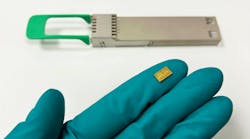
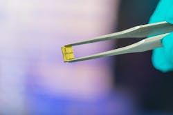
With SHIP validated on Tower’s production platform, customers now have a clear path from evaluation to high-volume manufacturing. Scintil used SHIP to move DWDM beyond a lab curiosity to a commercial product that can be manufactured at scale on the same lines manufacturing tens of millions of pluggable optical transceivers today.
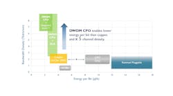
If you treat energy per bit, latency, and bandwidth per fiber as first-order metrics, then you need a DWDM-native source that fits existing SiPho flows. We’re moving from roadmap language to production reality.
LFW: How cool is it to see CPO take off?
Crowley: It’s not just a cool technology—it’s a paradigm shift in terms of AI data center architecture and economics. CPO is currently being deployed in scale-out networks, where it shows huge improvements in reliability, power consumption, and reach. But the scale-out is really just the test case for CPO, and the real revolution will come when CPO comes to the scale-up in 2028.
Compute is scaling rapidly and networking now gates performance. When you aggregate thousands of accelerators into coherent clusters, latency budgets and power per bit become structural constraints. Copper and front-panel pluggables can’t meet these constraints at scale.
CPO is where the physics and the packaging constraints point. Moving optics to the package boundary shortens electrical paths, lowers power, and increases channel density at the edge. This isn’t a trend driven by marketing, but rather by measurable system limits.
It’s exciting to see ecosystem alignment: Hyperscalers, processor vendors, foundries, and optical suppliers are converging on similar architectural choices. This convergence reduces uncertainty and accelerates deployment.
LFW: What do DWDM CPOs mean in terms of bringing photonics to the data center?
Crowley: DWDM CPO is a sort of holy grail technology for taking a huge collective of AI processors and memory and making it work like one gigantic chip. This will revolutionize the scale-up network and AI data centers in several ways: Lower power per bit; longer reach and larger scale-up clusters; lowest latency and tail latency to improve graphics processing unit (GPU) utilization in large clusters; and more bandwidth per fiber leads to bandwidth abundance.
Instead of adding more fibers to increase bandwidth, you increase the number of wavelengths per fiber to 8, 16, and beyond. It raises per-fiber throughput while controlling power and density. Long-haul telecom DWDM revolutionized the early internet by unleashing a flood of cheap bandwidth, and DWDM will have a similar impact in AI infrastructure as low-power, low-latency bandwidth becomes abundant and is no longer a performance bottleneck.
In practical terms, this means multi-terabit links at the package edge with lower energy per bit and tighter latency budgets. It enables a slow-and-wide network architecture that also allows simpler signaling at the electrical interface, which reduces reliance on heavy digital signal processing and deep forward error correction. It directly impacts tail latency and usable throughput.
For the data center, photonics becomes a foundational integration layer rather than an add-on module. It sits closer to the compute die and is aligned with the SiPho transceiver, and manufactured in flows that can scale to millions of units per month.
This is a structural shift in how optical technology participates in AI infrastructure.
LFW: How will this shake things up within the photonics industry?
Crowley: My career has involved taking bespoke manufactured products and moving them to wafer-scale monolithic manufacturing where you see massive improvements in reliability, manufacturing scale, cost, power, and features. SiPho has already had a huge impact in making photonics ubiquitous for AI data centers, and I suspect other industries will find new use cases and the industry will continue to expand.
It will make the photonics industry focus less on complex assembly and more on integrated single or multichip solutions. CPO already shows how advanced chipscale CPO allows photonics to merge with complementary metal-oxide semiconductors (CMOS) to create CPO solutions. Adding heterogeneous integration to this mix will allow the entire photonics signal chain to be copackaged into smaller form-factor, compact units.
Photonics companies will continue to look more like fabless semiconductor companies, and it will open up new markets beyond AI data centers (which is already mindbogglingly huge).
LFW: What’s next?
Crowley: For Scintil, next is disciplined execution. First, customer evaluations tied to specific DWDM CPO deployment plans. Now that our process flow development is complete, we have a toolkit to rapidly iterate designs and provide our customers with the exact frequency plan they need.
Second, we’re doing all of the things associated with a high-volume, high-quality product launch, such as qualifying our products, working with customers on internal demos, developing software for our custom application-specific integrated circuit (ASIC), and implementing all of our supply chain systems. This is where the upfront planning work ensures a seamless production ramp.
Third, we continue to invest in our roadmap. Moore’s Law is at its end, but the geometric increase in bandwidth DWDM can generate will be a new scaling law that can drive AI data center improvements for the next decade and beyond.