‘Optics when you must’ arrives for data centers
There’s a saying circulating around data center design: “Copper where you can, optics when you must.” For years, the pragmatic approach was to use cheap copper cables until physics forces you to upgrade. But as artificial intelligence (AI) clusters scale toward million graphics processing unit (GPU) “factories,” and data center economics come under pressure, we're learning “when you must” is arriving far faster than anyone expected.
Network architects already know that copper struggles with reach at high speeds. It’s less well understood why this happens at a fundamental physics level. Network engineers have brilliantly extracted every centimeter of reach and bit of bandwidth possible from copper. But physics always wins and no amount of brilliant engineering can overcome copper’s fundamental limitations. Once you understand this, the industry’s urgent pivot to copackaged optics (CPO) makes sense.
Higher-frequency electrical waves within copper enable higher symbol rates and bandwidth, which can carry more information. The problem is that as frequencies rise, reach falls. Two specific mechanisms are primarily responsible for this signal loss: the skin effect and dielectric loss.
Skin effect: When current betrays itself
When an alternating current (AC) signal travels through copper, the changing magnetic field induces eddy currents inside the conductor. These eddy currents create a magnetic field that opposes the signal’s magnetic field within the center of the wire. The faster the field changes, meaning the higher the frequency, the stronger this opposing effect becomes.
The consequence is that current gets crowded into a thin surface layer called the skin depth. At around 53 GHz—the frequency commonly used for current AI data center signaling—the skin depth is a mere 0.3 µm. At this thickness, using less than 1% of the conductor’s cross-section resistance explodes and can be more than 100x higher than its direct current (DC) resistance.
Dielectric loss: When insulation isn't free
Another major culprit behind signal degradation in copper is dielectric loss. At gigahertz frequencies, molecules within the dielectric can't keep moving fast enough to keep up. The lag between rapid field changes and molecular response to the field change converts electromagnetic energy from signal to heat.
A combined assault on data
When the skin effect and dielectric loss effects combine, it creates larger and larger losses at higher and higher frequencies. As an illustrative example of a possible loss budget at 50 GHz over 2 meters of cable, these mechanisms together can consume more than 90% of your signal power budget with high-quality cable. The physics of copper requires a fundamental tradeoff: bandwidth vs. reach.
CPO wins
The properties of optical transmission are fundamentally different from those of copper. Optical signals have no drifting electrons to jostle, far fewer degrees of freedom to lose energy, and much slower entropy accumulation per meter.
Photons are simply better at staying organized over distance, and it’s why copper signal reach is measured in meters, fiber in kilometers, and free-space optical in light years.
CPO was developed to confine copper primarily to ultrashort-reach, high-bandwidth links within an advanced copackaged form factor, while using optics for longer reaches. In CPO, copper is confined to ultrashort electrical paths, typically chip-to-chip with an interposer, while optical links carry traffic outside the package. Most communications leaving the CPO assembly run through optical fibers that can transmit data from meters to a few kilometers with very low loss.
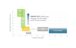
DWDM CPO
AI training clusters are now limited more by bandwidth requirements than by floating-point operations per second (FLOPS). In a scale-up network with coherent memory, new networking technology is needed that meets several criteria: Lower energy per bit as power becomes a limiting factor for data center deployment; more bandwidth per processor as FLOPs are no longer the bottleneck; higher density as the physical space needed to attach fibers becomes a limit; longer reach so scale-up domains can cross multiple racks; ultralow tail latency to keep memory domains coherent and improve GPU utilization; and high reliability and serviceability.
When tail latency is the binding constraint, meeting these requirements would unlock substantial gains in GPU utilization (with some models showing more than a doubling), materially reduce network power consumption, and improve end-to-end model performance. Today, dense wavelength-division multiplexing (DWDM) CPO is the most credible path we see to meet these constraints simultaneously. And the economic impact on hyperscalers will be profound.
DWDM CPO uses multiple wide and slow channels per GPU by running multiple wavelengths of light over each fiber strand. By increasing the number of wavelengths from 1 to 8, then to 16, and beyond, this geometric scaling law is poised to revolutionize AI networking just as telecom DWDM revolutionized internet backbones 25 years ago.
DWDM channels run slow at around 50 to 64 Gbit/s—low enough that engineers can simplify data encoding from PAM4 to NRZ (modulation techniques). This simplification eliminates several expensive, power-hungry signal-processing steps, reducing power and latency by simplifying the signal path.
Tail latency is the silent killer of data center return on investment (ROI). When a GPU cluster is processing tokens, it requires a continuous and predictable flow of bits into the cluster. When a single bit is delayed, the rest of the cluster is left idle, killing processor utilization. As the number of processors in a cluster increases, the probability of a p999 tail bit delay increases, and utilization decreases.
Without low-latency, low-power, long-reach DWDM CPO, networks are limited in size, which also limits large language model (LLM) performance. Larger, flatter, low-latency scale-up networks enable larger key and value (KV) caches, which directly increase the context window size and relevance, effectively making the LLM’s effective working memory larger. Increased low-latency bandwidth also has the potential to increase the number of transformer layers and enable deeper thinking and reasoning. In short: Reducing communication limits between chips will allow the LLM to retain more information in working memory and take more reasoning steps without stalling.
Copper was a great technology for its time, but fundamental physical limits in copper have generated an urgent need for more advanced networking technologies to massively improve hyperscaler ROI and expand LLM capabilities. In a few years’ time, the idea of an all-copper AI data center will be as inconceivable as an all-copper long-haul internet.
Hyperscalers, investors, LLM model developers, and other participants in AI infrastructure buildouts must be aware of this trend, as it promises to radically shift data center economics and expand AI capabilities. Early adopters of DWDM CPO technology are positioned to build architectural advantages in cost, power, and performance that will compound as AI infrastructure scales.
Related Article
About the Author

Matthew Crowley
Matthew Crowley is CEO of Scintil Photonics (Grenoble, France).