High-power Laser Diodes: Die-bonder innovations target HPLD manufacturing challenges

High-power laser diodes (HPLDs) are one of the fastest-growing types of lasers, primarily driven by the growth in their demand as pump sources used in fiber lasers that have emerged as the tool of choice for materials processing applications. HPLDs are also widely used directly in medical applications such as photodynamic therapy, cosmetic procedures, and tissue surgery, as well as direct-diode materials processing, which comprises cladding, 3D printing, cutting, and welding.
Another application area for HPLDs is the defense industry where their growth is driven by directed-energy weapons. HPLDs offer a wavelength range unmatched by any other laser type ranging from 400 to 2000 nm with an optical output range of one to more than 300 W delivered with the highest electrical-to-optical (E-O) conversion efficiency (up to 65%) in the most compact footprint.1 Single-emitters can deliver reliable optical output power up to 20 W in a 0.5 × 5 mm footprint.2
As a result of this unique set of capabilities, HPLDs fit into a broad range of applications underpinning their growth. According to the report “Laser Diodes & Direct Diode Lasers 2019-2029: Technologies, Markets & Forecasts” by analyst Dr Nilushi Wijeyasinghe, the global market for laser diodes and direct-diode lasers will reach a size of $13.985 billion by 2029, where laser diodes account for $11.952 billion and direct-diode lasers account for $2.033 billion.
Critical process challenges
The die bonding process is the most critical packaging step in HPLD manufacturing. During this process, a HPLD die in a form of either a chip or a bar is attached to a heat-sink substrate using a gold-tin (AuSn) eutectic bonding process. The joint between the die and the heat sink is typically AuSn solder using a eutectic bonding technique. The HPLD die can be single-emitter chips or multiple-emitter bar laser die. Regardless, the die bonding process is very critical for the HPLD product’s optical efficiency and field reliability. Some challenges for this critical process include precision, eutectic quality, percent voids, and coplanarity, as well as high-mix, high-volume production.
HPLD has a high-precision position requirement between the light-emitting front facet of a chip or bar and the edge of the heat-sink substrate. Normally, the chip post-bonding results should have no recess from the front facet to the substrate edge and the overhang of the facet shall be less than 5–10 μm. To achieve this, the die bonding machine post-bonding accuracy should typically be less than ±2.5 μm. Both the laser die and the edge of the substrate may have less than 1 μm tolerance. Therefore, the machine’s placement accuracy must be less than ±1.5 μm.
As HPLD chip power increases, the single-emitter chips become longer, with some chip length-to-width ratios exceeding 10. The HPLD laser bars are particularly challenging because of the large bonding surface area that amplifies any imperfections in post-bonding characteristics such as percent voids and bar tilt angles.
1.5 μm high-speed die bonder
To address these die bonding process challenges for HPLD production, an ultrahigh-precision, high-speed, highly flexible, fully automated die bonding machine is needed. The machine requirements include accuracy less than ±1.5 μm, programmable bonding force, eutectic stage, and bond tip scrubbing (small motions along X, Y, Z with controlled force) features. Understanding these requirements, the MRSI-H-LD 1.5 µm fully automated die bonder was developed.
Targeted at HPLD die bonding process applications, the MRSI-H-LD die bonders achieve a machine placement accuracy of ±1.5 μm at 3 sigma (@3σ). Parallel processes improve the machine’s cycle time. Though highly application-dependent, the typical chip-on-submount (CoS) units per hour exceeds 150.
A programmable bonding head with the real-time closed-loop force feedback and adjustment enables delicate handling of III-V semiconductor components. For example, by programming force values per component type, HPLD manufacturers can ensure that each large high-power laser die type can be picked and placed with its unique programmed and controlled force.
Void-free eutectic process
In addition to placement accuracy, the temperature profile in the reflow process is very critical for the HPLD die bonding process. During the eutectic process, special care needs to be taken to achieve a thin, uniform, and eutectic interface with minimal voids between the die and the heat-sink substrate to dissipate heat effectively and uniformly. This requires the die bonding machine to have an accurate and uniform eutectic reflow temperature control for the whole bonding area.
The programmable uniform eutectic heating stage with a fast temperature ramp-up and ramp-down is required for the HPLD die bonding process, and the temperature during the dwelling period has to be very stable. The heating stage also must have the forming gas cover to prevent oxidation of the bonding surfaces for good wetting and an interface with minimal voids upon cooling.
For example, the die bonder provides a unique pulse-heated fast-ramp eutectic bonding stage which has forming gas under a cover with a 90–95% nitrogen-hydrogen mix that can be used to prevent oxidation of the bonding surfaces. A eutectic composition is used so that the eutectic bonding process temperature is minimized, which is typically around 315°C. The heating stage is programmable up to 400°C with uniform temperature in the working plate. The heating stage is designed for long-lasting stability.
A unique programmable scrubbing solution addresses the coplanarity challenge for minimizing voids in the solder joint by applying both vertical and lateral forces and motions to a device during its placement to a substrate. A library for customized XYZ-theta achieves coplanarity despite different chip and submount conditions, delivering near void-free process control.
Coplanarity control
Coplanarity between the HPLD chip or bar and the heat-sink substrate is very critical because it can affect the percent voids and induced stress. Therefore, lack of coplanarity can affect HPLD product performance and reliability.
Without good coplanarity control, a bar could have warpage commonly referred to as bar smile as a result of post-bonding residual stress built up in the bar,3 and a long chip could have nonuniform heat dissipation that would create thermal stress along single-emitter length. Consequently, the various sizes of single-emitter chips or laser bar chips need different bonding force and accurate force control during reflow time.
A specially designed self-leveling tool improves bonding force uniformity and forces out air reducing voids. By applying a uniform bond force across the entire die surface, a near void-free eutectic bond results, which offers high die-shear strength and improved co-planarity.
On-the-fly tool change
Currently, the HPLD industry is in a state of transition where manufacturers must manage this growth and complexity of form factors due to the lack of standardization. The industrial HPLDs—CoS and bar-on-submount (BoS) designed by different suppliers—have many variables. As a result, high-mix production is a challenge for HPLD manufacturing because HPLD packaging design has numerous form factors to fit a variety of different applications.
The die bonder enables on-the-fly tool change for processing parts of different shapes and sizes without tool changeover or downtime. The system delivers industry-leading throughput and flexibility capable of die bonding single emitter CoS, laser diode (LD) bar on submount, and laser diode chip on C-mount, as well as other HPLD packaging in one machine.
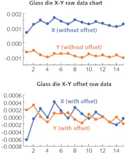
Experimental testing of the MRSI-H-LD die bonder was conducted using glass dies to assess the machine’s performance and verify equipment precision. The experiments included measuring the CoS and BoS die bonding process position accuracy, measuring the flatness profile of the HPLD bar, and scanning acoustic microscopy (SAM) to measure the percent voids.
The glass die experiment results, based on a sample size of 15 data points, yield a placement repeatability in the X and Y directions of less than 1 µm and 0.5 µm @3σ, respectively (see Fig. 1). In addition, the MRSI-H-LD die bonder features flip-chip functionality that enables completion of both P-side-up and P-side-down processes.
Chip-on-submount
For typical P-side-up CoS die bonding methodology process requirements, the critical CoS dimension, OH, for HPLD die bonding is the laser chip overhang (see Fig. 2) of A (emitter surface line) to C (AuSn surface line). The 10 test CoS build results show the post-bonding accuracy is less than ±3 µm @3σ, with no recess and overhang less than 4 µm.While placement repeatability, accuracy, and percent voids are vital performance metrics for HPLD die bonding, this capability must be delivered at high speed. A typical temperature profile is used for the eutectic die bonding process; the total cycle time is in the range of 23 seconds or greater than 150 units per hour (UPH).
Chip on C-mount
An overview of the experimental results obtained while bonding single-emitter LD chips on a C-mount package made of copper-tungsten (CuW) follows. In these experiments, an LD single-emitter chip measuring 2 mm × 500 µm × 0.12 µm was mounted to a C-mount package (with pre-deposited AuSn solder) measuring 6.35 mm × 2.18 mm × 6.86 mm (L × W × H). The results of chip placement on C-mount from a nine-sample build shows overhang less than 4.3µm @3σ, delivering key post-bonding placement parameters well within target specifications.
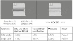
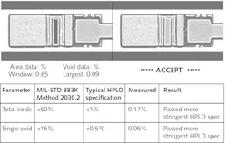
In addition to placement accuracy, percent voids in the solder interface were also measured using SAM. The processed and raw image acquired with a Sonoscan D-9000 C-SAM measurement tool, and the table shows the percent-void results (see Fig. 4). Again, in this experiment, post-bonding percent voids exceeded both MIL-STD 883K Method 2030.2 and a more-stringent HPLD specification.Laser bar on submount
An overview of HPLD bar packaging results of HPLD bars mounted on a CuW submount with pre-deposited AuSn solder follows. The HPLD bar used in this test measures 10 mm × 2 mm × 130 µm (L × W × H) and the CuW submount measures 10.6 mm × 4.0 mm × 0.25 mm (L × W × H).
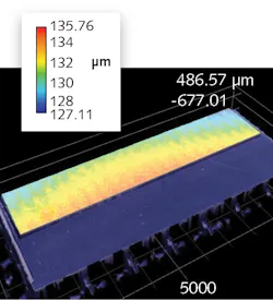
MRSI-H-LD features a self-leveling tip that preserves coplanarity of the laser die to the submount by applying uniform pressure across the entire bonding surface area to reduce the smile effect. A flatness profile of the mounted laser bar (see Fig. 5) shows that the front facet edge where laser radiation is emitted has a flatness is in the range of 130 µm ±1 µm or a mechanical smile range of less than 2 µm, which is acceptable for AuSn eutectic bonding.A low smile bar delivers a higher beam quality and therefore is a critical specification for all high-power applications. Linear offset or yaw across the length of the LD bar is an important parameter because the focused beam size of the LD bar will vary as a result of this offset.4 Typically, the edge-to-edge linear offset of a laser bar should be less than 5 µm. Based on the results of the experiment, linear offset measurements are 3.8 µm @3σ, which is well within specification.
Summary and conclusions
The experiments’ results show that the MRSI H-LD die bonder provides a perfect flexible manufacturing system (FMS)solution to address all of the die bonding process challenges for HPLD. The machine glass die precision is less than 1 µm @3σ, better than the 1.5 µm @3σ specification, and the overhang for CoS and Chip on C-mount is less than 4 µm and 4.3 µm, respectively.
In addition, the linear offset for bar-on-submount is 3.8 µm, which exceeds the less-than 5 µm specification. The void percent testing results show that the machine exceeds percent-void specifications for the eutectic process for all three package types. CoS, Chip on C-mount, and BoS packages can be built within one machine. With cycle times that achieve greater than 150 UPH for a typical CoS, the unique combination of features provides a perfect FMS die bonding solution for high-volume and high-mix HPLD packaging production.
REFERENCES
1. V. Rossin et al., “Chapter 5: Laser Diode Basics and Single-emitter performance,” High-Power Laser Handbook, Injeyan, Goodno-McGraw Hill (2011).
2. H.-G. Treusch and R. Pandey, “Chapter 6: High-Power Diode Laser Arrays,” High-Power Laser Handbook, Injeyan, Goodno-McGraw Hill (2011).
3. X. Liu et al., “Chapter 4: Thermal Stress in High Power Semiconductor Lasers,” Packaging of High Power Semiconductor Lasers, Springer Science (2015).
4. P. Loosen and A. Knitsch, “Chapter 4: Incoherent Beam Superposition and Stacking,” High Power Diode Lasers: Technology and Applications, Springer Science Series (2007).
About the Author
Limin Zhou
Senior Director of Strategic Marketing, MRSI (Mycronic Group)
Dr. Limin Zhou is senior director of strategic marketing at MRSI Systems (Mycronic Group), Tewksbury, MA.
Jack Inocencio
Customer Service Manager, MRSI (Mycronic Group)
Jack Inocencio is Customer Service Manager at MRSI (Mycronic Group), Tewksbury, MA.
Julius Ortega
Senior Applications Engineer, MRSI (Mycronic Group)
Julius Ortega is Senior Applications Engineer at MRSI (Mycronic Group), Tewksbury, MA.
Jason Liu
Customer Support Engineer, MRSI (Mycronic Group)
Jason Liu is customer support engineer at MRSI (Mycronic Group), Tewksbury, MA.


