Lasers for Lidar: Monolithic multichannel laser moves automotive lidar toward practical use
The driving force behind nearly all of today’s autonomous vehicles is the extraordinary, high-powered lasers driving lidar (light detection and ranging) systems. Lidar, featuring infrared lasers, navigates autonomous vehicles by creating a real-time, 3D image of the world. Pulsed lasers, along with single-pixel sensors or high-powered laser flash illumination using time of flight (TOF) cameras, are used to create the 3D images. The system measures the travel time of laser light from the autonomous vehicle to the target and back to the vehicle.
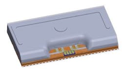
With increased laser power, 3D maps can capture more objects and scenery from longer distances, which is an attractive feature for lidar manufacturers. However, eye safety is a primary concern, so extremely short pulses are critical. Rapid pulsing (more than 1 million times per second) produces more data points and better signal quality, as the signal-to-noise ratio is proportional to the square root of the number of pulses)—as a result, fast rise and fall times are essential. Recently, Osram and GaN Systems (Kanata, ON, Canada) worked together to deliver lidar laser power with a performance of 120 W per channel in a four-channel SMT package delivering >480 W peak power with approximately 2 ns full-width half maximum (FWHM) pulses and <1 ns rise and fall times (see Fig. 1).
Why 905 nm monolithically spaced lasers?
As lidar has evolved, two primary wavelengths of consideration have emerged: 905 and 1550 nm. Both have their strengths. 905 nm is detectable using a CMOS or other silicon detector, thereby significantly reducing cost and complexity. Silicon photomultipliers (SiPMs), and eventually indium gallium arsenide (InGaAs) detectors, are typically used for 1550 nm detection, but present significant challenges at the 105°C temperature needed for automotive qualification. Eye-safety concerns are significantly reduced at 1550 nm—however, as recently seen at CES 2019,1 sensor damage in a consumer DLSR camera was observed. This occurred while using the typical kilowatt level of optical energy—an energy density that is still too low, as the triple junction configuration (three p-n sandwiched layers) needed to reach higher energy densities has yet to be implemented in that wide-bandgap crystal structure. High absorption of optical power is also observed at 1550 nm for the fog, snow, and rain that are part of an autonomous driving environment (see Table 1).2 In addition, multichannel lasers are very desirable: using eight lasers in individual firing will result in 1% resolution or 15 cm steps, whereas the minimum amplitude and dynamic range is approximately 18 dB when using a 1 ns time of flight. Clearly, there are significant advantages to using 905 nm multichannel high-power lidar lasers with nanosecond pulses.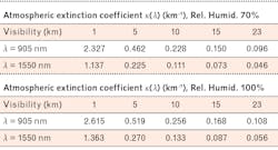
Osram’s 905 nm surface-mount chip is a monolithic array of four individual InGaAs/GaAs strained-quantum-well lasers, which can be driven individually or simultaneously with no optical crosstalk within the array due to the isolating v-grooves. When driven simultaneously, the output of the four channels combine to appear as one high powered laser pulse of 480 W (see Fig. 2). The definition of photodiode responsivity R(λ) is the ratio of generated photocurrent (IDP) to incident light power (PLight) using an InGaAs photodetector (Thorlabs DET08) to measure the incident pulse length. The incident light power at a given wavelength is defined as:


Monolithic lasers, which are tightly spaced, can lead to potential inductance coupling during simultaneous operation due to the proximity (<500 µm) of traces (current paths) connecting the individual channels. The increasing flow rapidly changes and the high current through small traces subjected to the inductance of the copper traces opposes the change in electric current. This effect is further exacerbated with greater rates of change, thereby making shorter pulses more difficult to achieve. The change in current induces a reverse voltage and a small magnetic field is created around the traces of the four channels. According to Faraday’s Law of induction, any change in magnetic flux through a circuit will induce an electromotive force measured in voltage across the circuit. This ratio between the induced voltage and the changing current in the traces is defined as inductance. With the inrush of current, according to Lentz’s Law, an induced voltage known as “back EMF” occurs in the opposite direction of current flow. This increasing opposition with shorter pulses presents a genuine challenge when considering the proximity of the neighboring lasers.
Wide-bandgap semiconductors
Osram engineers initially attempted to solve this problem by using a closely spaced silicon field-effect transistor (FET) to allow current to flow through the laser diodes during turn-on. This approach did not work. It did not matter how close the driver was to the laser diodes for this high-power product because silicon breaks down at the high current and bus voltages (>200 V) necessary to overcome inherent bond-wire inductance. Silicon FETs also display significant gate capacitance, which limits short-pulse operation. Lastly, incorporating the driver into a laser package is also not ideal from a passive thermal management perspective, as water cooling or thermoelectric coolers (TECs) are not cost-effective options in automotive applications.
The electric vehicle and optical communications industries have enjoyed the benefits of wide-bandgap semiconductors (where >2 eV of energy is needed to excite an electron into the conduction band) for years in very fast switching and high-powered battery charging circuits. Silicon (1.1 eV) was not able to meet this demanding performance due to having a low bandgap and the subsequent pitfalls.4 Silicon carbide (SiC), a common wide bandgap (3.2 eV) semiconductor, also does not offer the high electron mobility needed for fast switching (see Table 2), although it does exhibit superior thermal performance.
Gallium nitride (GaN) is a great blend of key attributes and is a wide bandgap semiconductor that can deliver the performance at automotive qualified temperatures with very high electron mobility (see Table 2). In addition, both SiC and GaN exhibit high critical field values, thus preventing breakdown and reduced leakage current. GaN thermal conductivity (about 3.5X that of silicon at 300K), high electric-field breakdown strength (about 15X that of Si for GaN) and wide bandgap (about 3X that of Si) make it a material ideally suited for high-temperature, high-power, and high-frequency environments. GaN is the ideal material to make a high-powered, fast-switching FET that can be actuated to allow current to flow through four high-powered laser channels simultaneously for the desired 480 W of optical power in a short pulse. Osram started a partnership with GaN Systems because of this research, as it offered the ideal GaN FET for driving four-channel lasers.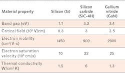

Receiver considerations
Lidar-detected range accuracy can be approximated as signal width divided by signal-to-noise ratio (SNR) after filtration and at not necessarily optimal conditions. Best detection performance occurs when the signal is filtered from noise (high SNR) while introducing minimal distorting to the received width pulse. This is best achieved by using a “whitening” matched filter, or other filters having the same principle.
Generating such an optimal filter (analog or digital) requires estimation of signal and noise at imperfect conditions such as received signal amplitude, pulse width, and smear resulting from tilted substrate reflections, noise, and background radiation, Johnson, and 1/f noise. Pulse scattering in aerosols creates a continuous DC back-reflection into the receiver that translates into shot noise. This reflection can also saturate the receiver in extreme conditions and, as a result, recovery time could be a few meters, therefore creating challenging receiving conditions.
It is apparent that matching the receiver to detect very short pulses may not be optimal in challenging conditions, as the wider receiver spectrum will introduce more noise into the final processed signal. Therefore, a hybridized mode consisting of short transmitted pulses with a slightly longer duration receiver “window” offers a more-robust system.
With the incorporation of further strategic partnerships, shorter pulses will be enabled for optimal eye safety and thermal management, as well a high resolution. The longstanding barrier of lidar technology has been the ability to transmit laser light in short pulses while maintaining high peak power. This hurdle has now been overcome, moving the technology one step closer to making autonomous driving a reality for everyone.
REFERENCES
1. See http://bit.ly/OsramRef1.
2. J. Wojtanowski et al., Opto-Electron. Rev., 22, 3, 183–190 (2014).
3. J. Williams, “AN98 Signal Sources, Conditioners, and Power Circuitry – Circuits of the Fall, 2004: Nanosecond Pulse Width Generator,” Linear Technology Corporation (2004).
4. See http://bit.ly/OsramRef4.
5. A. Mizan, H. Mousavian, and X. Cui, U.S. Patent Application No. 15/988,453 (2019).
About the Author
Ann Russell
Senior Applications Engineer, Osram Opto Semiconductors North America
Ann Russell is senior applications engineer at Osram Opto Semiconductors North America (Sunnyvale, CA).
Yochay Danziger
CTO, Lumus
Dr. Yochay Danziger is the CTO at Lumus (Ness Ziona, Israel), where he develops state-of-the-art, waveguide-based near-eye displays. Yochay participated in developing lidar systems and imaging systems, including thermal and VIS. These systems incorporated signal processing methodologies for detection and image reconstruction. Yochay received his PhD at the Weizmann Institute of Science, where he developed single-high-order-mode laser resonators.