Making nanostructures with a small EUV system
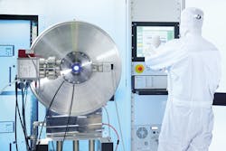
When the new iPhone hit the market in November 2020, it was fitted with a special processor made by extreme-ultraviolet (EUV) radiation at a wavelength of 13.5 nm (see Fig. 1). Research on EUV lithography has been carried out for decades, and now a machine can be purchased for over 100 million euros from ASML in The Netherlands. For smartphones with sales worth billions, such investments may pay off.
However, those who qualify EUV components or who just make some surfaces with nanometer structures may turn to a smaller solution. Scientists at the Fraunhofer Institute for Laser Technology (Fraunhofer ILT) and at the RWTH Aachen University (both in Aachen, Germany) have developed a technology producing periodic nanostructures using a proprietary EUV source and a relatively simple process technology.
The team used a holistic development approach: “It is important for us to be able to offer the complete process chain,” says project manager Serhiy Danylyuk from Fraunhofer ILT. “That’s why we have set up all the processes in-house, from simulation to mask production and the quality control of produced layers and nanostructures.” This way, the high-end technology becomes accessible to interested medium-sized companies or even startups at reasonable investment costs.
Near-field interference
The technical background for the method is based on interference effects of coherent radiation, such as the achromatic Talbot effect. In the near field—that is, <500 μm behind a mask—an intensity distribution is created with which microlithographic structures can be produced. The principle also works with relatively broadband radiation.
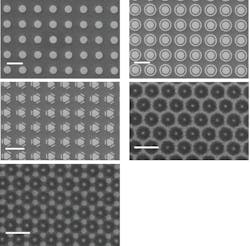
In simulations and laboratory tests, the Aachen-based company has optimized the process for EUV radiation at 13.5 nm. The depth of focus at a distance of 50 µm is then about 15 µm; this is well enough to process layers of a few hundred nanometers. The process can be used to generate both periodic line and hole structures. The holes can be rings or triangles—in principle, there is hardly any limit to the shape of the structures. In the imaging process, a transmission mask is magnified twice and imaged onto the wafer.
EUV source for structures smaller than 100 nm
The quest for a reliable source of EUV radiation has been ongoing for three decades; it was decisive for the whole process. In the end, laser-generated plasmas have been selected for the industrial manufacturing process. In particular, for the test of mirrors or resists, such devices are much too big.
Another technology for generating EUV could not scale to the powers needed for production processes, but for smaller tasks it is just right. Experts at Fraunhofer ILT have developed a beam source based on gas discharge that generates pulses with a power of up to 40 W in ±1% bandwidth. Power and spectrum are continuously monitored at the source, and the available intensity in the mask plane is more than 0.1 mW/cm2.
The processing of 1 mm2 takes about 30 s; a stitching of the processing areas is possible. Wafers with a diameter of up to 100 mm are processed in the Fraunhofer ILT facility. In the test, structures with a size of 28 nm (half pitch) could be produced using the achromatic Talbot effect, which is a world record for such a small system. The physical limit of the process is a structure size of 7.5 nm (half pitch). The error rate is low because the interference structures are inherently uniform.
More power with a deep-UV laser
In their laboratory, the Aachen-based research institute also tested the method with a KrF excimer laser at 248 nm. The LEAP150K laser system from Coherent delivers 1 J per pulse at 150 Hz. With this device, silicon can be ablated on glass; the structure sizes are then towards several 100 nm. For example, 180-nm-wide lines with a period of 600 nm were generated in photoresist. In addition, this technology is well suited for the ablation of PET plastic surfaces on a 300 nm scale.
Focus on medium-sized companies
Periodic nanostructures have different applications. They can be used in the optical industry as broadband antireflection coatings or polarizers, or in medicine and biotechnology as nanoscale particle filters. In electronics and metrology, they can be utilized to create novel sensor elements.
The new technology makes it possible to create the necessary geometries and structures; computational lithography methods are used for this purpose (see Fig. 2). Of course, the system can also be used to test parts of industrial EUV systems—for example, mirrors, photoresists, or other parts.EUV lithography is one of the most complex technologies ever developed. Just recently, the Wall Street Journal commented on EUV: “If Intel is a few years behind, China’s lag may be closer to a decade.”
European research efforts in EUV technology started more than 20 years ago; Fraunhofer ILT participated early. Together with other Fraunhofer Institutes, coatings with the highest degrees of reflection have been developed in addition to the pulsed beam source. For this, the renowned Joseph von Fraunhofer Prize was awarded in 2012. In November 2020, a collaboration from Zeiss, TRUMPF, and the Fraunhofer Institute for Applied Optics and Precision Engineering (Fraunhofer IOF) won the prestigious German Future Prize from the German Federal President for EUV lithography. After all, the technology has arrived in industry—and now, it is even available as a large or small solution.
About the Author
Andreas Thoss
Contributing Editor, Germany
Andreas Thoss is the Managing Director of THOSS Media (Berlin) and has many years of experience in photonics-related research, publishing, marketing, and public relations. He worked with John Wiley & Sons until 2010, when he founded THOSS Media. In 2012, he founded the scientific journal Advanced Optical Technologies. His university research focused on ultrashort and ultra-intense laser pulses, and he holds several patents.
Sascha Brose
Group Manager, EUV Technology at the Chair for Technology of Optical Systems, RWTH Aachen University
Sascha Brose is Chair for Technology of Optical Systems at RWTH Aachen University (Aachen, Germany).
Serhiy Danylyuk
Team Leader, EUV and DUV Technology at Fraunhofer ILT
Serhiy Danylyuk is Team Leader, EUV and DUV Technology at the Fraunhofer Institute for Laser Technology (Fraunhofer ILT; Aachen, Germany).


