DARPA PIPES Program demonstrates 2 Tbit/s optical interconnects at the chip level
A cooperative effort between researchers at Intel (Santa Clara, CA) and Ayar Labs (Emeryville, CA) has spawned the successful demonstration of high-bandwidth optical I/O interconnects that consume a small fraction of power compared to conventional electrical data links. The demo is a milestone in the Defense Advanced Research Projects Agency (DARPA) program entitled Photonics in the Package for Extreme Scalability (PIPES), established with the ambitious goal of developing advanced in-package silicon photonic interfaces capable of bandwidths greater than 100 Tbit/s at energies less than 1 pJ/bit, capable of kilometer-scale distances and more than 10x better performance compared to today’s state-of-the-art commercial interconnects at 400 Gbit/s.
Data communication propagates over optical fiber systems and networks until hitting a bottleneck at copper interconnects, the fundamental point-to-point conductive components on microchips and circuit boards. While optical transceivers are common today between servers and switches in data centers, electrons still transmit data relatively slowly across copper pins and wires from point to point on a circuit board.
Replacing copper with optical signaling is the next logical step in keeping up with Moore’s Law, but it's fraught with challenges. For high-bandwidth transmission, the maximum achievable interconnect distance falls off dramatically and energy efficiency decreases. Heat dissipation is also a problem at high bandwidths and increasing energy densities. Ayar Labs and Intel are striving to overcome this long-standing bandwidth-energy-distance tradeoff to push the demands of Moore’s Law beyond its original limits.1
In a live demonstration at the Optical Fiber Conference 2020 (which Ayar Labs participated in virtually during March 10-12 due to COVID-19), Ayar demonstrated its TeraPHY optical chip technology integrated into an advanced commercial integrated circuit (IC) that traditionally transmits electrons via copper: Intel’s Stratix 10 field-programmable gate array (FPGA). Ayar’s TeraPHY chiplet, containing micron-scale optical waveguides and photonic microring features, was fabricated using the 45-nm-platform CMOS chip manufacturing technology at GlobalFoundries (Santa Clara, CA).
Optical waveguides on the TeraPHY chip are patterned monolithically into the silicon, and are essentially the optical analog of copper wires. Bringing two waveguides in close proximity enables the transfer of photons and thus power from one waveguide to another to create an evanescent coupler. Within the coupler, a 10-µm-diameter microring resonator can electrically modulate the phase and control the direction of the light either through or up to the top of the chip, creating drop ports. Currently, most silicon-photonic chips use a 0.5-mm-sized Mach-Zehnder interferometer (MZI) to control direction and modulate the phase of the photons, which has limitations in bandwidth density and energy efficiency. Because this microring has a 100X smaller footprint than a typical MZI, it enables a 25 to 50X higher bandwidth density and 50X better energy efficiency. Such improvements effectively eliminate the traditional bandwidth/energy/distance limitation.
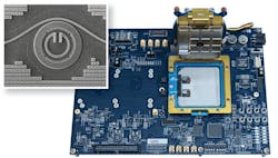
The single-die-package demo featured eight wavelength-division-multiplexed channels each at different wavelengths, with I/O data rates of 16 Gbit/s across four optical macro-chips, for a total of 512 Gbit/s. In production, the DARPA team expects the capacity of a single chiplet to reach up to 2.56 Tbit/s I/O over 24 channels with no forward error correction required and less than 10 ns latency (see figure). The TeraPHY optical interconnect is designed to work with an off-chip multiwavelength continuous-wave (CW) laser source and integrate with any type of partner system-on-package: CPU, GPU, ASIC, or FPGA, to connect switches, servers, and cards over distances up to 2 km.
To market and beyond
Ayar Labs, which spun out of the Massachusetts Institute of Technology in 2015, has received strategic funding from Intel Capital and GlobalFoundries, along with Silicon-Valley-based venture capital firms Founders Fund and Playground Global. The TeraPHY photonic interconnect launched commercially in 2019 with a target of solving the bottleneck problem in silicon chips; Ayar hopes to target other applications in supercomputer architecture, datacenters, and perhaps eventually in consumer electronics and autonomous vehicles. In March 2020, Lockheed Martin (North Bethesda, MD) agreed to provide Ayar with strategic funding of an undisclosed amount to spur commercialization of the TeraPHY technology. The next step for the group is to ramp up high-volume manufacturability.
In spite of this early-stage progress, the metrics needed to reach the goals of DARPA PIPES Phase 1 have a long way to go and longer still before 100 Tbit/s optical I/O reaches maturity. In March, DARPA announced the selection of research teams for the second technical area of the PIPES program proceeding simultaneously. The goal of the second research is to develop chips with petabit/second data rates, which is the equivalent of the entire aggregated traffic of the Internet today, on one chip. The researchers selected for this PIPES program funding include Sandia National Laboratories; University of California, San Diego; University of California, Santa Barbara; Columbia University; and the University of Pennsylvania. The teams will explore advances in signal efficiency, bandwidth density, and integration required to push 100X more data than today’s modern chips.
REFERENCE
1. R. Meade et al., "TeraPHY: A High-density Electronic-Photonic Chiplet for Optical I/O from a Multi-Chip Module," Optical Society of America Technical Digest, M4D.7 (Mar. 2019); https://bit.ly/TeraPHY.
About the Author

Valerie Coffey-Rosich
Contributing Editor
Valerie Coffey-Rosich is a freelance science and technology writer and editor and a contributing editor for Laser Focus World; she previously served as an Associate Technical Editor (2000-2003) and a Senior Technical Editor (2007-2008) for Laser Focus World.
Valerie holds a BS in physics from the University of Nevada, Reno, and an MA in astronomy from Boston University. She specializes in editing and writing about optics, photonics, astronomy, and physics in academic, reference, and business-to-business publications. In addition to Laser Focus World, her work has appeared online and in print for clients such as the American Institute of Physics, American Heritage Dictionary, BioPhotonics, Encyclopedia Britannica, EuroPhotonics, the Optical Society of America, Photonics Focus, Photonics Spectra, Sky & Telescope, and many others. She is based in Palm Springs, California.