Integrated Photonics: Hybrid integrated photonics cultivate a value chain
Big datacenters, Industry 4.0, and personalized healthcare—all these rapidly growing markets have one thing in common: they need miniaturized photonic components. Such miniaturized, or integrated, photonic components offer solutions for sensing, data transmission, and data processing.
The technologies for manufacturing, alignment, and assembly of integrated photonic components are evolving. Often, the markets are small—and so are the manufacturers—and, therefore, investments in individual solutions rather limited. Therefore, a number of concerns must be addressed to enable further development of this promising technology.
First, the development of new integrated photonic components has to apply existing processes either from the semiconductor or telecom industries whenever possible. Both industries have established large-scale production processes and realize considerable margins with it. We all have seen the advent of fiber lasers for materials processing, a development that was based on technology for telecom components.
Secondly, the growing community of mostly small- and medium-sized enterprises (SMEs) that is working on photonic integrated components can seek governmental and private funding to accelerate the technology development. Of course, this has to be application-driven; taxpayers and their political representatives insist on that.
It is certainly helpful that the entire trend of integrated photonics fits into the bigger picture. At a recent event of the German Fraunhofer society, the CEO and president of the Carl Zeiss group, Michael Kaschke, predicted the “integration and convergence of optical and electronic functions” as one of the major technical trends for the next 20 years. As a simple example, one may look at the case of datacenters, where electrical and even fiber connections have already reached their limits. The problem has been well known for more than a decade, but it is now that integrated photonic solutions for racks, boards, or on the chip level are conquering this market.
And finally, one can think about integrated photonics as an investment. The market for integrated photonics might be fragmented and consist of many small niches, but for most players commodification is far away. Proficiency pays off for decades here.
The PolyPhotonics Berlin project
Within the Berlin, Germany area the development of telecom components and other photonic integrated components has a long history. A whole ecosystem with research institutions and small, medium or even larger companies has evolved over the years. In 2016, this was one reason that the German Federal Ministry of Education and Research (BMBF) funded a so-called “Innovative Regional Growth Core” to push integrated photonics technology development in this area.
This program provided funding of 9 million Euro for a network of 14 partners (who contributed another 4 million Euro) with a total of 22 projects over three years. Under the name “PolyPhotonics Berlin,” the network intended to lift the technology from a range of separate ideas toward a vertically integrated value chain for a wide range of products. This includes a superior material system, automated assembly lines, and global marketing to reach out to new markets (see Fig. 1).
On October 24, 2019, the PolyPhotonics consortium met in Berlin to discuss the outcome of the project. The meeting (as well as the project management) was hosted by the Fraunhofer Heinrich Hertz Institute. Its director, Martin Schell, took the audience on a journey through 20 years of integrated photonics development.
When looking at the various proposed materials, such as indium phosphide or silicon, he concluded it would desirable to replace them with polymer technology. Polymers transmit more wavelengths, and polymer-based components can be produced in smaller batches with higher margins.
The core technology of the PolyPhotonics projects is a modular technology platform for integrated photonics. At the core of the platform is indeed a polymer chip with optical waveguides. This chip may feature passive elements such as optical fibers, thin film filters, isolators, rotators, and micro-optics. Photodiodes and laser systems can be added as needed. These components are connected to the waveguides via microfabrication procedures.
The members of the PolyPhotonics consortium developed not only appropriate material solutions and integrated components; some partners also came up with customized design and simulation procedures, as well as automated manufacturing and alignment systems. A fully automated production system can be seen in a video at http://bit.ly/PolyPhotonics.
Applications
In addition to technological solutions, the consortium members created a set of basic building blocks for integration of photonics into compact functional modules (hybrid integration). They developed systems for telecom or datacom applications such as multiplexers, 10G or 100 GE transceivers, tunable lasers for terahertz or analytical applications, and interrogators for fiber-Bragg-grating sensor systems.
One particular example is a sensor for measuring strain in wind-turbine blades. Physically, it measures transmission changes in a fiber Bragg grating (FBG). Three partners have developed a new module to process the signals from the fiber sensors in the turbine blades. They added electronics and performed all tests. Considered in terms of a marketing and sales strategy, it helps one of the players to turn from a pure component provider towards a system provider.
A second example came from a local provider of sophisticated laser-diode technology. For each of its laser diodes, the provider sells between 100 and 10,000 pieces per year. As the CEO said, “These devices just turn electrical current into light.” But often customers need more, namely systems with additional components such as isolators or nonlinear optics. The PolyPhotonics project helped the company to build a laser diode with a tunable gain chip, allowing it to offer a wavelength-tunable narrow-bandwidth laser source based on the use of a polymer grating.
In the audience at the final project workshop were not only project partners; one could also spot people from the growing space-satellite business, where small and reliable modules will always find interest.
What’s next?
A few things are generally discussed at the end of most funding projects: What has been learned? Can the results be transferred into marketable products and, anyway, what’s next?
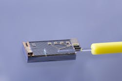
The first thing learned was that it takes a lot of persistence and a good caterer to get through all the communication efforts and the paperwork successfully. Secondly, the transfer into real products is happening. The partners are selling products based on the PolyPhotonics toolbox, such as the transceiver shown in Figure 2, successfully.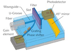
The question of what next steps to take is more complex. The funding agencies involved see a success and will turn to other objectives that might be accessible for the partners. The project participants themselves have decided to establish a PolyPhotonics Association—financed by its members, this association will act as point of contact for customers and engage in common marketing efforts.
About the Author

Andreas Thoss
Contributing Editor, Germany
Andreas Thoss is the Managing Director of THOSS Media (Berlin) and has many years of experience in photonics-related research, publishing, marketing, and public relations. He worked with John Wiley & Sons until 2010, when he founded THOSS Media. In 2012, he founded the scientific journal Advanced Optical Technologies. His university research focused on ultrashort and ultra-intense laser pulses, and he holds several patents.