Silicon photonics fabrication now uses latest CMOS process
In 2015, a team of researchers led by groups at the Massachusetts Institute of Technology (MIT; Cambridge, MA), the University of California at Berkeley, and Boston University (BU) announced a milestone: the fabrication of a working silicon (Si)-based microprocessor, built using only conventional CMOS manufacturing processes, that integrated electronic and photonic components on the same chip. The researchers’ approach, however, required that the chip’s electrical components be built from the same layer of Si as its photonic components. That meant relying on an older CMOS technology in which the Si layers for the electronics were thick enough for optics. Now, a team of 18 researchers, led by the same MIT, Berkeley, and BU groups, has developed a technique for assembling on-chip photonics and electronics separately, which enables the use of more modern CMOS manufacturing processes.
The earlier work on integrated photonics involved wafer bonding, in which a single, large crystal of Si is fused to a layer of glass deposited atop a separate chip. The new work, in enabling the direct deposition of Si with varying thickness on top of glass, must make do with polysilicon (poly-Si). While single-crystal Si is useful for both optics and electronics, in poly-Si there’s a tradeoff between optical and electrical efficiency. Large-crystal poly-Si is efficient at conducting electricity, but the large crystals tend to scatter light, lowering the optical efficiency. Small-crystal poly-Si scatters light less, but it’s not as good a conductor. Using the manufacturing facilities at SUNY-Albany’s Colleges for Nanoscale Sciences and Engineering, the researchers tried out a series of recipes for poly-Si deposition, varying the type of raw Si used, processing temperatures and times, until they found one that offered a good tradeoff between electronic and optical properties.
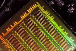
In addition to millions of transistors for executing computations, the researchers’ new chip includes all the components necessary for optical communication: modulators, waveguides, resonators, and photodetectors. Reference: A. H. Atabaki et al., Nature (2018); doi:10.1038/s41586-018-0028-z.
About the Author

John Wallace
Senior Technical Editor (1998-2022)
John Wallace was with Laser Focus World for nearly 25 years, retiring in late June 2022. He obtained a bachelor's degree in mechanical engineering and physics at Rutgers University and a master's in optical engineering at the University of Rochester. Before becoming an editor, John worked as an engineer at RCA, Exxon, Eastman Kodak, and GCA Corporation.