Hamamatsu Photonics introduces the iPHEMOS®-DDX inverted emission microscope for failure analysis of advanced semiconductor packages
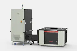
BRIDGEWATER, N.J., Oct. 1, 2026 /PRNewswire/ -- Hamamatsu Photonics has developed the iPHEMOS®-DDX, an inverted emission microscope designed for failure analysis of advanced semiconductor packages, including AI chiplets, High Bandwidth Memory (HBM), 2.5D/3D packages, and large-scale semiconductor packages.
The semiconductor industry is rapidly advancing with the growth of generative AI, driving increased performance in AI chips while making device structures increasingly complex and highly miniaturized. As package structures become more complex, identifying failure locations becomes increasingly difficult, creating demand for highly accurate and efficient failure analysis technologies such as the iPHEMOS®-DDX inverted emission microscope.
The iPHEMOS®-DDX system enables flexible integration into existing tester-centered measurement environments by supporting direct docking to testers from three directions. In addition, it integrates seven analysis techniques—PEM, Thermal/LIT, LSM, OBIRCH, DALS, EOP/EOFM, and TD Imaging—into a single platform, which can improve failure analysis workflows and reduce analysis time.
Hamamatsu will showcase this new failure analysis system at ISTFA 2026, to be held in San Antonio, Texas, from October 4 through October 8.
For more information about the iPHEMOS®-DDX inverted emission microscope, including pricing and delivery time, please visit the company's website, https://www.hamamatsu.com or call Hamamatsu Corporation at (908) 231-0960.