Photodiodes: Graphene photodetector has 50 GHz speed and high responsivity from 0.6 to 20 μm
Conventional semiconductor photodiode materials (silicon, indium gallium arsenide, mercury cadmium telluride, and so on), while extremely useful in photonics, have sensitivities that span only small portions of the visible/infrared (IR) spectrum. (Mercury cadmium telluride is a special case: by varying the proportion of cadmium to mercury, its bandgap can be tuned from 400 to 14,000 nm, but the resulting fabricated device still has a relatively narrow bandwidth.) In addition, achieving a fast-enough temporal response to produce bandwidths in the tens of gigahertz is difficult for conventional semiconductors.
Graphene, in contrast, has optical and electronic characteristics that lead to very broadband performance and ultrahigh speeds when used as a photodiode. It can absorb energy from a broad swath of the electromagnetic spectrum, from the ultraviolet through visible light to the infrared and microwave bands. Unfortunately, graphene has an optical absorption of only about 2% across this spectrum, and in addition has a very short photocarrier lifetime, leading to very low electrical current.
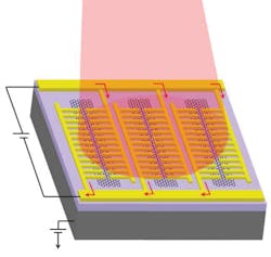
Now, a group at the University of California Los Angeles (UCLA) has augmented the photodetection capabilities of graphene by forming it into nanostripes connected to patches of gold (see figure).1 The resulting device has very broadband sensitivity, with a responsitivity ranging from 0.6 A/W at a 0.8 μm wavelength to 11.5 A/W at 20 μm. In addition, the detector is ultrafast, operating at speeds up to 50 GHz.
To form the photodetector, the researchers laid strips of graphene over a silicon dioxide layer, which itself covers a base of silicon. Then, they created a series of comblike nanoscale patterns made of gold, with teeth about 100 nm wide. The total area of the photodetector was 30 × 30 µm2. The gold-patched graphene nanostripes achieve carrier multiplication, resulting in a boost to the photoconductive gain at shorter wavelengths. The structure also boosts optical absorption, especially at longer wavelengths. The combination of effects results in the detector’s improved performance.
The spectral responsivity of the detector was measured using an optical power of 2.5 μW, a gate voltage of 25 V, and a bias voltage of 20 mV. The demonstrated operation shows the widest photodetection bandwidth with the highest responsivity to date, say the researchers. The asymmetric form of the gold-patched graphene nanostripes produces a high sensitivity to the polarization of the incoming light, which the researchers say can lead to applications in polarimetric sensing and imaging.
“We specifically designed the dimensions of the graphene nanostripes and their metal patches such that incoming visible and infrared light is tightly confined inside them,” says Semih Cakmakyapan, a UCLA postdoctoral scholar and the lead author of the study. “This design efficiently produces an electrical signal that follows ultrafast and subtle variations in the light’s intensity over the entire spectral range, from visible to infrared.”
425 GHz photoresponse cutoff frequency
The researchers say that the ultrafast 50 GHz photodetection speed is because of the subpicosecond photocarrier transport times in the gold patches while at the same time maintaining low capacitive and resistive parasitics, resulting in a predicted photoresponse cutoff frequency of 425 GHz.
“Our photodetector could extend the scope and potential uses of photodetectors in imaging and sensing systems,” says Mona Jarrahi, a professor of electrical and computer engineering, who led the study. “It could dramatically improve thermal imaging in night vision or in medical diagnosis applications where subtle differences in temperatures can give doctors a lot of information on their patients. It could also be used in environmental sensing technologies to more accurately identify the concentration of pollutants.”
REFERENCE
1. S. Cakmakyapan et al., Light Sci. Appl. (2018); https://doi.org/10.1038/s41377-018-0020-2.
About the Author

John Wallace
Senior Technical Editor (1998-2022)
John Wallace was with Laser Focus World for nearly 25 years, retiring in late June 2022. He obtained a bachelor's degree in mechanical engineering and physics at Rutgers University and a master's in optical engineering at the University of Rochester. Before becoming an editor, John worked as an engineer at RCA, Exxon, Eastman Kodak, and GCA Corporation.