Advances in Detectors: Graphene photodetectors advance with help from collective EU Flagship
SOPHIA LLOYD
Graphene is a stable allotrope of carbon, in which carbon atoms are arranged in a single-atom-thick hexagonal lattice. Groundbreaking experiments on the fundamental physics of graphene led to the 2010 Nobel Prize for Andre Geim and Konstatin Novoselov. With remarkable electronic, optical, thermal, and mechanical properties, graphene is promising for applications including flexible electronics, high-frequency electronics, energy generation and storage, composite materials, and optoelectronic devices.
In 2013, the European Union (EU) launched the Future and Emerging Technology Graphene Flagship to accelerate research into new technologies based on graphene and related materials (GRMs) including layered transition metal dichalcogenides and new materials such as silicene and phosphorene. More than 150 industrial and academic partners across 23 European countries are participating in this 10-year, $1.13 billion project, aiming to transform laboratory research into commercially viable technologies based on GRMs.
Graphene is particularly attractive for optoelectronics applications, including telecommunications components, terahertz antennas and detectors, lasers, plasmonic sensors, and photodetectors. Its gapless electronic structure leads to extremely broadband optical absorption, and its high carrier mobility enables ultrafast response times. Graphene's compact nature, high room-temperature mobility, and compatibility with silicon mean that these functions can be integrated into on-chip platforms, without the need for bulky optics and cooling systems.
Despite its single-atomic thinness, graphene absorbs 2.3% of incident light. There are several different mechanisms for photodetection for graphene-based devices, including photovoltaic current generation, bolometric conductance changes, the photothermoelectric effect, photogating using external photoabsorbers, and plasma-wave assisted detection.1 The Graphene Flagship is exploiting these mechanisms in graphene-based photodetectors across different frequency ranges to advance a variety of commercial applications.
Infrared imaging and spectroscopy
Using graphene as a conductive channel and a separate sensitizing layer is a promising route towards fast, broadband imaging sensors. The optical response of the sensitizing layer can be tuned, while the excellent electrical properties of graphene enhance the overall responsivity of the detector.
A specific target is hyperspectral imaging in the visible to shortwave-infrared (SWIR) range, which is important for security, night vision, and machine vision applications. Very high responsivity hyperspectral detectors also have potential for spectroscopy with high spectral resolution.
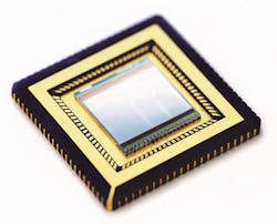
Working with graphene production company Graphenea (San Sebastian, Spain), ICFO (Barcelona, Spain) demonstrated graphene-quantum dot photodetector arrays fully vertically integrated into a CMOS chip with read-out integrated circuits (ROICs; see Fig. 1).2 These 388 × 288 pixel cameras are the first to operate in the UV-visible-SWIR range from 300 to 2000 nm.
Based on a photogating effect, the photodetector array has high gain of 107 and responsivity of 108 A/W—significantly higher than the 0.5 A/W responsivity of an image sensor based on lead-sulfide (PbS) colloidal quantum dots, for example. Reference pixels exhibited a dynamic range of >80 dB and response time <1 ms suitable for frame rates over 1000 frames per second (frames/s). However, the performance of the camera was limited by the off-the-shelf ROIC.
Emberion (Espoo, Finland), a research and development company spun out of Nokia, is developing a range of complementary metal-oxide semiconductor (CMOS) integrated photodetectors operating in the visible-SWIR spectrum based on graphene transducers and optically active crystalline nanomaterials. These application-specific detector arrays are integrated with custom ROICs to exploit the full capabilities of these graphene-based detectors.
Beyond the visible-SWIR region, graphene-based detectors are also enhancing imaging and spectroscopy in the mid-infrared (mid-IR) region. The University of Cambridge (Cambridge, England) and Emberion demonstrated mid-IR photodetectors with high sensitivity-capable of detecting the presence of a human hand from 15 cm away.3 The detector consists of a graphene channel over a pyroelectric substrate that is heated through light absorption. A floating gate electrode concentrates the pyroelectric field over the graphene channel, enabling detection via bolometric principles.
By tuning the sensitivity and spectral response through the pixel size and geometry, small detectors down to 20 × 20 μm2 are suitable for high-spatial-resolution thermal imaging, while the high sensitivity of larger detectors opens up possibilities for spectroscopy in the mid- and far-IR with high spectral resolution. Operating at room temperature, the sensitive spectrometer could be useful in hazardous material and gas detection applications.
Terahertz imaging
The frequency range between 0.1 and 10 THz is of increasing importance for security screening, non-destructive testing and defect analysis, chemical sensing, and biomedical imaging. These applications are driving the need for fast and sensitive terahertz components that are portable and can operate at room temperature.
Dyakonov and Shur proposed a mechanism for detection of terahertz radiation based on plasma waves propagating in a 2D electron gas field-effect transistor (FET). Graphene FETs have since been demonstrated by CNR (Rome, Italy) and the University of Cambridge to be suitable for both resonant and broadband terahertz photodetectors.4
In a typical plasma-wave-assisted graphene photodetector, the source and gate electrode of a graphene FET are connected to the lobes of an antenna, directing the terahertz signal into the sub-wavelength area of the FET and generating plasma waves in the graphene. Resonant detection occurs when the plasma waves travel across the FET channel in a time shorter than the momentum relaxation time generating a source-drain photovoltage, while overdamped plasma waves give broadband detection.
Research from CNR, IIT (Genoa, Italy), and the University of Cambridge demonstrated bilayer graphene FET terahertz detectors with high responsivities of 1.2 V/W or 1.3 mA/W and low noise, competitive with commercial terahertz detectors.5 Furthermore, terahertz detectors based on epitaxially grown graphene on silicon carbide from CNR and Fondazione Bruno Kessler (Trento, Italy) are promising for scalable fabrication of integrated detectors and large-area detector arrays for imaging, although further work is needed to boost the responsivity and noise performance to be commercially competitive.6
Other GRMs are also being studied for applications in terahertz detection. Black phosphorous is a layered material consisting of stacks of phosphorene, in a similar manner to graphite and graphene. Unlike graphene, phosphorene is not atomically flat, but instead has a ridged structure that leads to an inherent anisotropy in its electronic transport properties and a bandgap that depends on the number of layers.
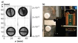
Black phosphorous-based terahertz detectors have been shown to have low noise and very high responsivity of 5.0 V/W for plasma-based detectors, and 7.8 V/W for bolometric detectors.7 The potential for these high-responsivity terahertz detectors has even been demonstrated in quality control applications (see Fig. 2).Telecommunications
Fueled by the rise in connectivity and the Internet of Things, the demands on optical communications systems are rapidly increasing, with current technologies reaching the limits of speed, bandwidth, and power consumption. Next-generation telecommunications systems must be able to cope with high volumes of traffic, while also reducing energy consumption by increasing efficiency.
Graphene is promising for high-speed and energy-efficient optical communications applications because of its high mobility and low intrinsic noise. Graphene has been measured to have an intrinsic data bandwidth of 262 GHz, and recent results are confirming this potential.8 AMO (Aachen, Germany) and Vienna Technical University (Vienna, Austria) reported waveguide-integrated photodetectors with high-cutoff data frequencies of 65 GHz, which indicates a potential data rate of around 90 Gbit/s.9 In these detectors, light is guided into a slot waveguide by silicon strip waveguides that also act as local gate electrodes, inducing a p-n junction in graphene over the slot waveguide.
So far, the highest reported bandwidth for a graphene-based photodetector is 76 GHz, corresponding to a data rate of 100 Gbit/s.10 However, the bandwidth of these bolometric photodetectors from AMO was limited by the measurement setup, meaning the bandwidth of the detectors could potentially be higher.
Graphene-based Schottky diodes, in which single-layer graphene is inserted between the metal and silicon interface, can operate at significantly higher efficiencies than standard metal-silicon Schottky photodiodes. In collaboration with the Hebrew University of Jerusalem (Jerusalem, Israel) and John Hopkins University (Baltimore, MD), the University of Cambridge reported waveguide-integrated Schottky photodetectors with enhanced responsivity and high internal quantum efficiency of 7% compared to <1% in silicon-based diodes (see Fig. 3).11 Such improvements demonstrate graphene's potential to deliver higher-efficiency operation with sensitivities at or above the state-of-the art in silicon photonics—essential for technological integration.Graphene-based detection and modulation platforms can also be integrated onto the same chip, taking advantage of graphene's high conductivity to provide fast detection and modulation, as well as high data rates. The Graphene Flagship is developing a prototype transceiver bank based on active components as a key deliverable of its optoelectronics research program.
Scaling detector technologies
Photodetection platforms based on graphene are highly promising in terms of operation speed, sensitivity, and frequency range. To be competitive with existing technologies, the new photodetectors must be produced at low cost and high volumes, and offer enhanced energy efficiency (for example, in telecommunications). Alternatively, they could open up brand-new opportunities that do not otherwise exist (such as in CMOS-integrated hyperspectral and terahertz imaging).
Many of these recent research and development results rely on graphene obtained via chemical vapor deposition (CVD) or mechanical exfoliation and transferred onto wafers. The challenge is now to implement this approach in CMOS fabrication processes, both in obtaining large-area, high-quality graphene and in the transfer process, which can induce defects or misalignment.
Groups within the Graphene Flagship are exploring several potential routes to integration of graphene with integrated electronic and photonic circuits. The first applications of graphene-based optoelectronics are arising through post-processing and back-end-of-line processing, in which graphene is transferred onto pre-fabricated circuits.
Emberion is using this strategy to integrate their custom-designed ROICs with graphene-based photodetectors. A promising route to high-mobility graphene for wafer integration is CVD growth on copper foils seeded with chromium nanoparticles, producing single-crystalline graphene in controlled arrays that can be transferred onto wafers and etched.12 Alternative approaches, such as the direct growth of graphene onto insulating silicon carbide wafers, could be suitable for front-end-of-line processes, though silicon carbide wafers are relatively expensive.
By engaging with industry partners from production, through proof-of-concept, and into commercially viable technologies, the Graphene Flagship's approach creates a strong foundation from which graphene photodetector development is rapidly advancing.
REFERENCES
1. F. H. L. Koppens et al., Nat. Nanotechnol., 9, 780–793 (2014).
2. S. Goossens et al., Nat. Photon., doi:10.1038/nphoton.2017.75 (2017).
3. U. Sassi et al., Nat. Commun., 8, 14311 (2017).
4. L. Vicarelli et al., Nat. Mater., 11, 865–871 (2012).
5. D. Spirito et al., Appl. Phys. Lett., 104, 061111 (2014).
6. F. Bianco et al., Appl. Phys. Lett., 107, 131104 (2015).
7. L. Viti et al., Sci. Rep., 6, 20474 (2016).
8. A. Urich et al., Nano Lett., 11, 2804 (2011).
9. S. Schuler et al., Nano Lett., 16, 7107 (2016).
10. D. Schall et al., J. Phys. D: Appl. Phys., 50, 124004 (2017).
11. I. Goykhman et al., Nano Lett., 16, 3005 (2016).
12. V. Miseikis et al., 2D Mater., 4, 021004 (2017).
Sophia Lloyd is the science writer for the Graphene Flagship, based at the Cambridge Graphene Centre at the University of Cambridge, Cambridge, England; e-mail: [email protected]; www.graphene.cam.ac.uk.


