Photonic Frontiers: Detectors and Sensors: Looking Back/Looking Forward: Detectors continue evolving to meet changing application needs

My first high-school experiment with light measurement was connecting an analog meter to a solar cell. I wasn't satisfied with the results, so I bought an inexpensive vacuum photodiode and persuaded a friend to build a drive circuit. He used vacuum tubes because they were easier than transistors to extract from the scrapped electronics we got on the cheap from Bickoff's junkyard in Newark. We never got it to work well, but it was an adventure.
The gold standard for optical measurements in the 1960s was the photomultiplier tube invented in 1934 by Harley Iams and Bernard Salzberg of RCA (Harrison, NJ). A byproduct of their work on television cameras, it combined the photoemissive cathode of a vacuum photodiode with one or more electrodes that amplified the signal by secondary emission of electrons. The founders of Hamamatsu TV, established in 1953, also came from a television background, and its early products included imaging tubes as well as photomultipliers.
Lasers and photomultipliers
Theodore Maiman connected a photomultiplier to an oscilloscope to measure pulses generated by the first ruby laser, using a filter to block ambient light and avoid overloading the tube. He recorded scope traces with a Polaroid camera, and estimated accuracy at within 10%.1 Other laser researchers followed in his footsteps, creating a new market for photomultipliers and vacuum photodiodes.
Two detectors made our first New Products column in the January 1, 1965 issue. One announced that ITT Industrial Laboratories (Fort Wayne, IN) had designed vacuum photodiodes with "excellent saturation, rise-time and linearity" to detect laser radiation. Their S-1 response from 300 to 1200 nm covered the outputs of ruby, helium neon, and neodymium lasers. The same page reported that Edgerton, Germeshausen and Grier Inc., (Boston, MA) could customize packaging of its SD-100 semiconductor photodiodes for applications including laser systems.
Detectors often were only footnotes in stories about new laser systems. Our August 1, 1965 issue described the diode laser transmitter for the Gemini 7 spacecraft in great detail, but all it said about a crucial photomultiplier was that it was a cooled RCA model 7102 with an S-1 photocathode. Detector speed was important for optical communications, so on November 1, 1965, we reported that cryogenic cooling and bathing photoconductive germanium at RCA Laboratories (Princeton, NJ) had raised bandwidth to 100 MHz—enough to carry up to 25 television channels.
Solid-state detectors
By September 1974, solid-state detectors had the lead for optical communications through fiber or through air (see Fig. 1). Forrest M. Mims wrote that PIN photodiodes were the least expensive detectors, but that avalanche photodiodes (APDs) had a higher gain-bandwidth product. Yet APDs were limited by temperature sensitivity, high operation voltages, and high noise, so the most promising approach was a module containing a detector, amplifier, and other electronics.
Our January 1975 issue covered a diverse variety of solid-state infrared (IR)detectors. Barnes Engineering (Stamford, CT) advertised several: indium-antimonide for high sensitivity at 3–5 µm, lead-tin-telluride for 8–12 µm, pyroelectric detectors for room temperature, thermistor bolometers for long wavelengths, and thermopiles, gold-doped germanium, and indium arsenide for other uses. Mercury-cadmium-telluride (HgCdTe) had emerged from an early veil of military security, with fast photovoltaic detectors with quantum efficiency above 30% being advertised by Eltek Corp. (Larchmont, NY). Oriel Corp. of America (Stamford, CT) offered photon-drag detectors with nanosecond response for use with CO2 lasers. And Optical Engineering Inc. (Santa Rosa, CA) advertised "laser imaging surfaces" to view IR beams as an alternative to "smoldering paper, perforated popsicle sticks, and glowing fire bricks."
A decade of progress in both optical communications and HgCdTe were evident in our October 1984 issue. Our fiber-optic section reported that 1.3 µm systems used InGaAs or germanium PIN photodiodes, and that InGaAs APDs were in development for future systems. RCA advertised 250 MHz InGaAs PIN diodes with spectral range of 900 to 1700 nm packaged with an integral hybrid preamplifier. M/A-COM Laser Diode advertised a digital receiver for up to 500 Mbit/s, above the 400 Mbit/s of early singlemode backbone networks. Judson Infrared (Montgomeryville, PA) advertised single diodes or arrays of photoconductive HgCdTe, packaged with glass and metal dewars or thermoelectric coolers.
Self-calibrating detectors and computer interfaces for radiometers were the two biggest trends in optical radiation measurements. "The self-calibrated detector is now a standard for use over the visible spectrum," replacing source-based calibration, wrote William E. Schneider, president of Optronic Laboratories (Orlando, FL), in the October 1984 issue. "Self-calibrated quantum detectors also make very accurate measurements." He added, "Computer-controlled measurement systems can now accomplish measurements in a few minutes that just a few years ago involved hours of tedious, time-consuming manual data recording and reduction." That trend would continue as personal computers emerged and matured, eventually transforming optical measurements.
Our March 1990 technology guide to detectors mentioned photomultipliers briefly before describing silicon detectors at great length. It also covered a wide variety of IR detectors, including photoconductive lead selenide and sulfide at 1–7 µm, photovoltaic germanium at 0.8–1.8 µm, HgCdTe and related compounds with a potentially broad range, indium antimonide at 1.0–5.5 µm, InGaAs at 0.8–2.6 µm, thermopiles, and pyroelectrics. It noted that 90% of papers at the March 1989 SPIE Conference on Future IR Detector Materials were devoted to HgCdTe.2 Much of that work was on arrays, which I will cover in the July 2015 issue.Challenges of speed and integration
Photomultiplier tubes were getting on in years, but in the December 1995 issue executive editor Heather Messenger wrote that their fast response and sensitivity at low light levels earned them wide use in equipment from color scanners for printing to orbital telescopes. She described plans for the Pierre Auger Observatory, a massive array of 1600 stations spaced 1.5 km apart on the Argentine Pampa, each containing three PMTs in a tank. A second planned array was never built.
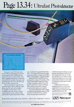
In our March 1995 issue, scientists from Picometrix (Ann Arbor, MI), a spinoff of the University of Michigan's center for ultrafast physics, told how they made and measured a detector with a record 7 ps response time, equivalent to 60 GHz of bandwidth. Their feat required shrinking the area and thickness of the absorption layer in a new detector based on low-temperature GaAs, without sacrificing too much light absorption or responsivity. Newport (Irvine, CA) marketed the new detector in an ad in the same issue (see Fig. 2).
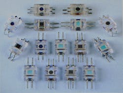
They developed the detector for use with ultrafast titanium-sapphire lasers, says Rob Risser, chief executive of the company, which renamed itself Advanced Photonix after a 2005 acquisition. Such high-speed detectors soon found another use—in high-performance test instruments for fiber-optic systems at 2.5 Gbit/s and later in the new generation of test equipment needed for 10 Gbit/s OC-192 systems.Higher speeds also increased the push for integrating detectors into receiver modules. One driver was cost reduction. Another was performance. As data rates and signal frequencies increased, constraints on electronic design and component size become tighter. The trend went well beyond fiber-optic systems. Many OEM customers were designing integrated assemblies rather than discrete detectors into their systems, Ken Sinclair of Advanced Photonix (then a separate company) wrote in our May 2000 issue. "These assemblies range from simple packages to fully integrated photodetection systems with sophisticated signal amplification and processing electronics." He cited applications ranging from measuring eyeglass prescriptions to high-performance particle counting systems. Figure 3 shows injection-molded detector assemblies, with dyes added to the plastic to filter undesired wavelengths.
Data rates above 10 Gbit/s required more advanced detectors. Our preview of the Optical Fiber Communications Conference in the February 2005 issue cited an integrated photonic circuit that Infinera (Sunnyvale, CA) used to receive 10 channels at 40 Gbit/s, for a total data rate of 400 Gbit/s. Also covered was unrepeatered transmission of 20 Gbit/s through 210 km of fiber using coherent detection and digital signal processing by the University of Tokyo.
Coherent detection requires additional signal processing in the receiver, making it an increasingly complex optical system. With 100 Gbit/s systems, described in our March 2010 issue, the input signal is split between eight parallel paths, reducing power per path, and requiring amplification before it can be processed extensively, says Risser. "Now our receiver looks like a complicated subsystem with photonic integrated circuits including eight detectors and an amplifier." Digital signal processing can clean up dispersion, but for a 100 Gbit/s coherent signal that requires silicon-germanium amplifiers with electronic speeds of 40–50 GHz, far beyond the 7–8 GHz needed for 10 Gbit/s signals. "So you're pushing the state of the art in electronic transistor technology," he adds.
New APD and photomultiplier technology
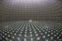
A feature in our April 2005 issue described a new twist on avalanche photodiodes that made them useful for single-photon detection. The devices, called "single-photon avalanche photodiodes" (SPADs), operate in Geiger mode, so each detected photon produces a pulse of electrons, and the entire pulse is counted as only one photon detected. Biased over the breakdown voltage, SPADs "are remarkably different from ordinary APDs," which operate as linear amplifiers slightly below breakdown, wrote Nick Bertone of Optoelectronic Components (Pierrefonds, QC, Canada) and colleagues.Vacuum photomultipliers remain a favorite for high-energy physics experiments because they can cover large areas at lower cost than silicon—important for detecting rare events such as the neutrinos sought by the Japanese Super-Kamiokande experiment, which holds over 11,000 photomultipliers in a tank containing 50,000 tons of highly purified water (see Fig. 4). A single photon can trigger the photomultipliers, says Earl Hergert of Hamamatsu. "That signal would be overwhelmed by dark noise in silicon."
The biggest challenge to vacuum photomultipliers today, he says, is the "silicon photomultiplier" (SiPM), which Hergbert and Slawomir Piatek described in our November 2014 issue. Invented in Russia, it's essentially an array of avalanche photodiodes operating in Geiger mode, like the SPADs described earlier. Counting the number of microcells that fire gives a pseudo-linear response. "APDs typically have gains of only a few hundred, but SiMTs have gains of 500,000 to one million," Hergbert says. Yet vacuum PMTs have lower noise than any silicon device, and are very fast for large devices.
Terahertz technology
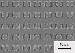
Recent advances in pyroelectric materials and coating, noise performance, and digital signal processing make pyroelectric detectors increasingly attractive for terahertz detection, wrote Don Dooley of Spectrum Detector (Oswego, OR) in our May 2010 issue. New pyroelectric detector performance can match or exceed that of traditional Golay cells.Antenna-like structures similar to terahertz emitters also function as terahertz detectors, with their output sampled at high frequency to reconstruct the signal. Our August 2014 issue described a promising approach, using carbon nanotubes to absorb the terahertz waves. Online, we described how a metamaterial antenna could absorb a terahertz signal and transfer it to a structure made of gallium arsenide or other materials (see Fig. 5).
With prices of terahertz equipment dropping, Risser sees a promising future for terahertz detectors in applications that require peering inside opaque objects to see internal structure and compositions. For example, they could spot flaws inside asphalt shingles before they cause problems on your roof. Volume production should reduce sensor prices. Applications will require libraries of characteristic signatures, so the system can identify hidden materials and structures by matching profiles rather than imaging the structures.
Looking forward
Trends such as continuing increases in coherent communication speeds pose other challenges. "The killer challenge" for emerging 200 and 400 Gbit/s coherent networks, Risser says, "is can you really get an electrical amplifier that runs at 60 GHz. You need 350 GHz transistors to make a 30 GHz linear amplifier, so you might need 500 to 550 GHz for a 60 GHz linear amplifier, and we're not there yet." So electronics could prove to be a key limit to optical coherent detection.
A broader change that has been coming for a long time is increasing the integration of detectors, Hergert says. "Instrument makers want things with digital output, smart sensors, that they can plug and it starts talking to the instrument." They want it to come with look-up tables and built-in diagnostics to schedule preventative maintenance and warn of potential failure. "It's not quite there yet, but it's coming for high-end detectors, maybe in five to ten years," he says.
The integration trend could also aid growth of a new class of "point-of-care" medical devices, such as a miniature blood chemistry lab for use in a doctor's office. Many blood tests are done optically, so miniaturized smart sensors could perform many tests on a single small blood sample. "The holy grail is a noninvasive blood glucose measurement" usable in the home, says Hergert. It's a very difficult problem, but it could be a boon for the treatment of diabetes. A new generation of smart and even more compact optical sensors will be needed for future smartphones and wearable devices.
REFERENCES
1. T. H. Maiman et al., Phys. Rev., 123, 1151 (Aug. 15, 1961).
2. J. W. Baars and R. E. Longshore, "Future Infrared Detector Materials," Proc. SPIE, 1106 (Mar. 27, 1989); see http://bit.ly/1Ha8gCv.
About the Author
Jeff Hecht
Contributing Editor
Jeff Hecht is a regular contributing editor to Laser Focus World and has been covering the laser industry for 35 years. A prolific book author, Jeff's published works include “Understanding Fiber Optics,” “Understanding Lasers,” “The Laser Guidebook,” and “Beam Weapons: The Next Arms Race.” He also has written books on the histories of lasers and fiber optics, including “City of Light: The Story of Fiber Optics,” and “Beam: The Race to Make the Laser.” Find out more at jeffhecht.com.
