Testing Detectors: Understanding key parameters of silicon photomultipliers
The silicon photomultiplier (SiPM) is becoming a popular photodetector choice in applications where even individual photons must be detected. Before development of the SiPM around 1990 by Russian physicists, a photomultiplier tube (PMT) would have been the only choice for a detector in very-low-light-level applications such as flow cytometry, radiation detection in particle and nuclear physics, or medical imaging.1
Although both PMT and SiPM detectors are now in direct competition, it is unlikely that SiPMs will make PMTs obsolete. Each detector has some distinct advantages over the other. For example, the PMT's large photosensitive area and very low noise make it superior in particle physics as used in the Super-Kamiokande project in Japan (see http://www-sk.icrr.u-tokyo.ac.jp/sk/index-e.html), whereas the SiPM's ruggedness and ease-of-use make it uniquely suitable for portable and handheld devices such as light detection and ranging (LIDAR) systems.
Using a SiPM in scientific and clinical research requires familiarity with its optical and electrical behavior under varied environmental conditions, the types and rates of noise, and the limits on reliable light detection. Although manufacturers of SiPMs provide information on their products, an independent check of the detector's characteristics—especially in critical situations where a scientific breakthrough hinges on the validity of the measurements—is advisable. Once basic operational principles of a SiPM are understood, readers can benefit from a review of select methods of characterizing and testing the device.
Equivalent circuit and operation
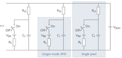
A SiPM is a two-prong photodetector consisting of identical pixels connected in parallel and arranged in a rectangular pattern. One pixel is a series combination of an avalanche photodiode (APD) operating in Geiger mode and a quenching resistor RQ. In typical operation, an external voltage source reverse-biases the SiPM to a voltage VBIAS that is up to a few volts greater than the breakdown voltage VBR of the APD. Depending on the design of a SiPM, VBR is in the 30 to 70 V range. An overvoltage ΔV ≡ VBIAS–VBR is one of the most important adjustable parameters affecting the performance of the detector, controlling its optical and electrical characteristics such as the gain (M), photon detection efficiency (PDE), the rates of dark counts, afterpulsing, and optical crosstalk.
For the equivalent electrical circuit of a SiPM, the APD consists of a capacitor CJ (representing the capacitance of the p-n junction), the ON/OFF switch, the voltage source VBR with terminal voltage equal to the breakdown voltage, and finally, the resistor RS representing the combined resistance of the p-n structure during an avalanche (see Fig. 1).
In the absence of light and ignoring dark counts, the switch in a pixel is in the OFF position and the voltage on CJ equals VBIAS (VBIAS > VBR), that is, the pixel is in a light-sensitive state. When a pixel absorbs a photon, an electron-hole pair forms, and one of the charge carriers drifts to the high-field (avalanche) region of the APD where it can initiate an avalanche.
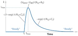
At the instant the avalanche begins, the switch in the equivalent circuit closes, causing CJ to discharge through RS (RS << RQ) with time constant RSCJ. The voltage on CJ decreases, reducing the probability of impact ionization in the avalanche region. For the appropriate choice of RQ, the probability becomes so small that the avalanche is quenched due to random fluctuations of the current. At the instant of quenching, the switch goes to the OFF position and VBIAS recharges CJ with a time constant RQCJ. The resulting current pulse—due to absorption of a photon by a pixel—flows through the terminals of the SiPM (see Fig. 2). The avalanche begins at ti and is quenched at tmax.Silicon photomultipliers are designed so that imax (referred to as the "latch" current) is ~20 μA. The condition for proper quenching is 0 < ΔV < RQimax. For ΔV = 1 V, the minimum RQ is 50 kΩ. If RQ is set below this limit, the quenching time increases, which shows as flattening of the current pulse around tmax. If RQ is substantially below the minimum limit, the quenching never occurs and the current becomes constant with an amplitude of (VBIAS - VBR)/(RQ + RS). The characteristic time for the rising edge of the pulse is ~1 ns and for the falling edge, ~10 ns.
Integrating the current pulse with respect to time yields the total charge Q that transfers between the terminals of the SiPM. Since a single charge carrier triggered the transfer, the gain M = Q/e. A detailed analysis shows that Q = CJΔV and, thus, M = CJΔV/e. If two or more pixels "fire" nearly simultaneously in response to incident light, the output current pulse is a linear superposition of two individual pulses; however, if a single pixel fires in response to two or more photons striking it simultaneously, the output current pulse is the same as that for a single photon. Therefore, a pixel can be thought of as a binary device that is either sensitive to light ("ready" state) or not ("off" state), and the transition from the former to the latter state produces the same output signal regardless of the number of simultaneously absorbed photons.
Characterizing a SiPM (measuring RQ, VBR, and CJ)
A current/voltage (I-V) curve of a SiPM acquired under dark conditions and at a fixed temperature provides information about RQ and VBR. Under increasing forward bias, the equivalent circuit of a single pixel converges to a series combination of RQ and RD, where RD represents the combined resistance of the APD's semiconductor structure having a typical value of hundreds of ohms. Because RQ >> RD, a SiPM with Npix pixels becomes equivalent to a parallel combination of Npix quenching resistors. Thus, the I-V curve becomes linear with the slope converging to Npix/RQ. By measuring the slope, one may then determine RQ.
Under increasing reverse bias and close to VBR, the monotonically rising current shows two sharp increases: the first occurs at VBR, and the second happens at a larger voltage for which latch current begins to flow through each pixel. Thus, the plot of dlog(I)/dV versus the reverse voltage shows two distinct peaks; the maximum of the one at the lower voltage is at VBR.
The effective capacitance seen at the terminals of a SiPM is NpixCJ. Because CJ is a function of reverse voltage, the Keithley C-V 590 analyzer or the Agilent 4980A LCR meter is well suited for determining this dependence. The resulting capacitance/voltage (C-V) curve shows that CJ decreases with increasing reverse voltage until the voltage at which full depletion occurs. For still higher voltages, CJ remains nearly flat even beyond VBR. The voltage for full depletion is several tens of volts below VBR.
Observing noise
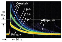
A SiPM generates output pulses in the absence of light due to 3 processes: dark counts, afterpulses, and optical crosstalk. These are noise. A thermally generated charge carrier that triggers an avalanche is responsible for dark counts. A signal due to dark count is indistinguishable from one that would have resulted from photon absorption. Dark counts are random and always present regardless of the light level illuminating the SiPM. Their rate increases with temperature and ΔV.
The incidence of after-pulsing and crosstalk is correlated with the occurrence of an avalanche triggered either by a photogenerated or thermally generated charge carrier. An afterpulse arises when a charge trap (such as a lattice defect) releases charge in a pixel that is recovering from a primary avalanche, and the released charge triggers a secondary avalanche. Here, the SiPM's output consists of a primary pulse convolved with the lagging secondary pulse. Optical crosstalk appears when the primary avalanche causes an emission of photons, which can trigger one or more avalanches in the neighboring pixels. The resulting output signal is an in-phase superposition of the pulses from all of the "fired" pixels.
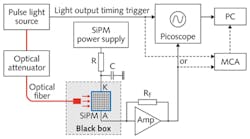
To observe noise, a block diagram of an "all-purpose" experimental setup can be used (see Fig. 3). For this purpose, the pulsed light source and optical attenuator are not needed; R is a safety resistor (about 1 kΩ), and capacitor C (about 0.2 μF) filters out AC noise from the biasing voltage. The setting of the power supply controls the value of ΔV and the output of the SiPM goes to the transimpedance amplifier, which converts the output current pulse to a voltage pulse that then goes to a picoscope (a PC-based oscilloscope).PDE is the product of quantum efficiency η, the geometrical fill factor Fg, and a combined probability Pa of electrons and holes initiating an avalanche; that is, PDE = ηFgPa. The value of η is a probability that a photon generates a charge carrier that enters the avalanche region. It is a function of the wavelength of light λ and temperature T, but it is independent of ΔV for full depletion. The geometrical fill factor Fg is a ratio of the combined photosensitive area to the total area of a SiPM. The avalanche probability Pa is a function of λ, T, and ΔV.
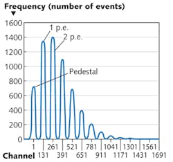
For a PDE measurement, the optical attenuator is adjusted so that the average number of photons per pulse, N¯γ, arrives at the plane of the SiPM. N¯γ must be measured using a calibrated detector such as a PMT. The picoscope or, alternatively, a multichannel analyzer, digitizes and integrates the signal to obtain a charge amplitude spectrum with an idealized form (see Fig. 5). Although the abscissa reads "Channel," it can be expressed by integrated charge Q or the number of detected photons.The probability P of detecting Npe photons by a SiPM is given by the Poisson distribution as follows:
Here, N¯pe is the average number of detected photons. The events for Npe = 0 (no photon detected) correspond to the "pedestal" on the charge amplitude spectrum; the subsequent peaks are for Npe = 1, 2, …
The values of P(Npe, N-pe) for Npe > 0 are distorted by the presence of crosstalk and afterpulsing, but the value for Npe = 0 is not. Measuring P(0, N¯pe), the ratio of the number of events in pedestal N0 and the total number of events NT, allows unbiased determination of N¯pe. Both N0 and NT are determined from the charge amplitude spectrum.
Since P(0, N¯pe) = N0/NT = exp(- N¯pe), then N-pe = -ln(N0/NT). Taking into account dark pulses, N¯pe = ln(N0/NT) + ln(N0D/NTD), where N0D and NTD are the number of events in the pedestal and the total number of events, respectively, in a charge amplitude spectrum taken under dark conditions. Thus, PDE = N¯pe/N¯γ. Repeating this procedure for different values of λ, T, or ΔV yields the dependence of PDE on these parameters.
A charge amplitude spectrum of a SiPM produced by a multichannel analyzer can also be used to find the gain M as
Here, QDCcal = charge/one channel of QDC (charge-to-digital converter); Δpp = number of channels separating two adjacent peaks; Kamp = amplification factor of the electronics; and e = fundamental charge value. If charge amplitude spectra are collected for various settings of VBIAS, M as a function of VBIAS can be found. Plotting M versus VBIAS yields a linear relationship with the slope and vertical-intercept equal to CJ/e and CJVBR/e, respectively. Therefore, fitting a straight line to the data gives the values of CJ and VBR.
Although this article reviews general methods of measuring key optical and electrical parameters of a SiPM, more detailed descriptions of experimental setups and procedures can be found.2-4
References
1. A. G. Gasanov et al., Lett. J. Technol. Phys. 16, 14 (1990; in Russian).
2. P. Eckert et al., Nucl. Instrum. Methods A 620, 217–226 (2010).
3. A. Vacheret et al., Nucl. Instrum. Methods A 656, 69–83 (2011).
4. M. Ramilli et al., Silicon Photomultipliers: Characterization and Apps, Photodetectors, ISBN: 978-953-51-0358-5 (InTech, 2012).
About the Author
Slawomir S. Piatek
Hamamatsu Corporation
Slawomir S. Piatek has been measuring proper motions of nearby galaxies using images obtained with the Hubble Space Telescope as a senior university lecturer of physics at New Jersey Institute of Technology. He has developed a photonics training program for engineers at Hamamatsu Corporation in New Jersey in the role of a science consultant. Also at Hamamatsu, he is involved in popularizing a SiPM as a novel photodetector by writing and lecturing about it, and by experimenting with the device. He earned a Ph.D. in Physics at Rutgers, the State University of New Jersey.
Earl Hergert
VP of Marketing, Hamamatsu
Earl Hergert is VP of Marketing at Hamamatsu (Bridgewater, NJ).
