Optical phased array enables lensless camera
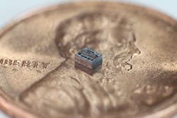
Over the past few years, Laser Focus World has written about numerous lensless imaging technologies, including a fiber-optic imaging endoscope, a coded-mask camera, and several variations of lens-free holographic technologies, including a holographic microscope for a smartphone and a combination of digital holography and optical coherence tomography (OCT) called holoscopy. Now, researchers at the California Institute of Technology (Caltech; Pasadena, CA) have developed a new lensless camera using an 8 x 8 optical phased array (OPA) receiver.
The receiver itself is an 8 × 8 on-chip array of grating couplers that capture the incident light and send it into 64 waveguides that route the light to a directional coupler, where it is combined with a reference beam in a heterodyne scheme. The reference beam is split into 64 paths that each enter a PIN diode phase shifter, and are mixed with the 64 input signals and fed into photodiodes. By adjusting the phase shift of each path, signals from certain directions add constructively while light from other directions is rejected. Scanning the beam and capturing light coming from all directions yields the image of the object in front of the chip. Using a 1550 nm source, the received beam width is 0.75° and grating lobes are 8° apart, enabling a lensless 8 × 8 or 64-pixel imaging camera from the OPA. Reference: R. Fatemi et al., CLEO 2017, paper JW2A.9, San Jose, CA (May 17, 2017); see https://goo.gl/goH32E.
About the Author

Gail Overton
Senior Editor (2004-2020)
Gail has more than 30 years of engineering, marketing, product management, and editorial experience in the photonics and optical communications industry. Before joining the staff at Laser Focus World in 2004, she held many product management and product marketing roles in the fiber-optics industry, most notably at Hughes (El Segundo, CA), GTE Labs (Waltham, MA), Corning (Corning, NY), Photon Kinetics (Beaverton, OR), and Newport Corporation (Irvine, CA). During her marketing career, Gail published articles in WDM Solutions and Sensors magazine and traveled internationally to conduct product and sales training. Gail received her BS degree in physics, with an emphasis in optics, from San Diego State University in San Diego, CA in May 1986.