Demand for high-speed detectors drives research
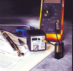
The demand for gigabit-speed fiberoptic communication and the rising popularity of fiberoptics in RF/microwave systems have led to many advances in high-speed photodetector technology. Specific application requirements have spurred development of novel device structures to improve the speed, responsivity, and power-handling capabilities of high-speed detectors. Simultaneously, advances in materials and processing techniques have made these developments possible. The fastest commercially available photodetectors have bandwidths of 60 GHz at visible wavelengths and 45 GHz at infrared wavelengths, with a typical maximum responsivity of 0.2 to 0.4 A/W (see photo). Despite this high performance available with traditional photodetector designs, efforts are underway to move beyond the fundamental limits of the photodiode.
This article discusses two classes of high-speed detectors that recently have received much attention—RCE (resonant-cavity enhanced) detectors, which can provide high-speed, high-quantum-efficiency detection and wavelength selectivity, and high-power traveling-wave detectors. These devices possess high optical saturation powers that allow analog fiber links to operate with less RF insertion loss, less noise, and larger spur-free dynamic ranges.
Resonant-cavity enhanced detectors
Traditional high-speed photodiodes are designed around a trade-off between bandwidth and responsivity. To achieve a high-bandwidth device, the transit time of the photogenerated carriers across the high-field depletion region must be held small, placing an upper limit on the absorption layer thickness. For most semiconductor devices operating in the tens-of-gigahertz regime, this limit becomes comparable to the absorption length of the absorbing material, which dictates significant sacrifice of responsivity to achieve high-speed operation. The RCE detector provides a means of sidestepping this trade-off by enabling layers much thinner than an absorption length to absorb nearly all of the optical power.
The basic RCE device consists of a thin—compared to an absorption length—narrow-bandgap absorbing layer positioned within a Fabry-Perot cavity (see Fig. 1). In addition to the absorbing layer, nonabsorbing spacer layers are included to permit adjustment of the total cavity length. Under resonant illumination, the intracavity intensity increases sharply so that the power dissipated in the absorbing layer becomes comparable to that in the incident beam. The internal quantum efficiency of the device approaches unity, significantly exceeding that obtained with a single pass through the absorbing layer. With RCE devices, responsivity is divorced from transit time.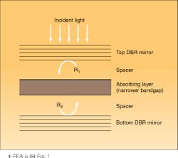
A second feature of the RCE detector is its wavelength selectivity. The off-resonant wavelengths are reflected, leading to very low responsivities. This characteristic makes the RCE detector a candidate for use in wavelength-division multiplexing. The presence of loss in the cavity, however, increases crosstalk between channels above what can be obtained with separate filters.
Yet another feature of the RCE detector is that it can be used to achieve low-voltage device operation. Because the depletion layer can be made thinner, designs requiring a lower voltage to deplete the absorbing layer are possible. This is particularly helpful in situations where a long absorption length would otherwise require thick depletion layers and high bias voltages. Low-voltage operation can be important for battery-operated devices.
Detector design
A comprehensive review of the design issues and trade-offs for RCE detectors has been published.1 Primary design parameters are the reflectivities of the cavity mirrors, the cavity length, the absorption layer thickness, and the position of the absorption layer within the cavity. The effective cavity length, which accounts for the optical field within the mirrors, determines the resonant wavelengths, while the peak quantum efficiency and the width of the resonant peak are determined by all of the cavity parameters. Particularly for thin absorbing layers, the position of this layer within the cavity can be important. The amount of power it absorbs will depend on whether it appears at a node or an antinode of the electric-field standing wave. Most often, an antinode is desired to increase absorption.
Fabrication of the RCE detector generally requires high-reflectivity distributed Bragg reflectors, and this places constraints on the material system used for the devices. Mirror materials should be low-loss and the index of refraction should be sufficiently different for each of the two alternating layers. Also, lattice matching between layers must be adequate. These requirements are best met by the gallium arsenide/aluminum gallium arsenide (GaAs/AlGaAs) material system that has been used in most work to date. For this system, mirror fabrication is aided by the large index difference between GaAs and AlAs—3.5 and 3, respectively. By using a strained InGaAs absorbing layer, operation can be extended beyond the band-edge of GaAs. Beyond a wavelength of about 1 µm, however, the strained-layer thickness becomes too thin for proper device performance.
High-performance devices
Much recent work has been directed toward obtaining high-performance devices capable of operating at communication wavelengths. Candidate material systems include indium phosphide/indium gallium arsenide/indium aluminum arsenide (InP/InGaAs/InAlAs), aluminum arsenide/gallium arsenide/germanium (AlAs/GaAs/Ge), and silicon/silicon germanium (Si/SiGe). While none of these systems possess properties as favorable as those of GaAs/AlGaAs, they do make possible RCE devices capable of operating at wavelengths up to 1.55 µm. The InP/InGaAs/InAlAs system has attractive material properties, although a larger difference in indices—3.45 for InGaAs, 3.2 for InAlAs and InP at 1.35 µm—would be preferable. A smaller difference in indices requires more mirror layers and a thicker overall structure, which presents greater challenges for the epitaxial growth.
A simulation has demonstrated the effect of resonant enhancement when a 100-nm layer with an absorption length of 1 µm, assumed wavelength-independent, is positioned between a bottom mirror with unity reflectivity and a top mirror with 70% reflectivity. The internal quantum efficiency of such a device, neglecting the mirrors, is roughly 10%. When the resonance is included, the efficiency exceeds 90% (see Fig. 2).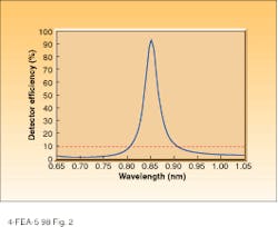
RCE detectors have been realized as p-i-n, Schottky, and avalanche photodiodes. A p-i-n device, constructed with an InGaAs/InP bottom mirror and substrate reflection for the top mirror, designed for 1.55 µm, relied on the bandgap shift of heavily doped InGaAs layers to reduce the absorption in the mirror structure.2 This mirror achieved a reflectivity of 97%, and the detector's peak quantum efficiency reached 65%, which represents an enhancement factor of four in responsivity over a conventional p-i-n diode with the same 200-nm InGaAs absorbing layer. A similar absorbing layer in an InGaAs/InGaAsP/InP structure with mirror reflectivities of 0.7 and 0.95 leads to a quantum efficiency of 82%.3
High-power photodiodes
To achieve good signal fidelity, analog fiberoptic links and interconnects often require low-noise, high-power lasers. Examples include optical beamforming for phased-array antennas and antenna remoting. Receivers in such systems must be capable of linearly detecting microwave-frequency, high-power optical signals. Most of the photodetectors available today are not capable of handling the requisite powers (10–100 mW), so several research groups are exploring means of improving the saturation powers of high-speed detectors.
The power-handling capabilities of high-speed photodiodes are limited by screening effects of the photogenerated carriers. When the carrier density becomes too large in the absorption region, the electric field is screened and carriers are no longer efficiently collected. Consequently, transit time is increased, slowing the device. For high-speed detectors, which have small active areas to minimize capacitance, power-handling capabilities decrease as the detector design bandwidth increases. Typically, for detectors operating above about 10 GHz, saturation occurs in the few-milliwatt regime.
To extend saturation powers to the 100-mW level, the absorbing volume must be made larger. To accomplish this, a single device cannot simply be made larger because increased transit time or capacitance will slow the device. Recently, a new type of photodetector structure for simultaneously achieving high saturation power and high speed has been demonstrated. The detector, known as the velocity-matched distributed photodetector (VMDP) achieves high power-handling capability by combining the outputs of multiple photodetectors. The combination maintains the speed of a single photodetector because the device capacitances are distributed along a transmission line in much the same way as a distributed amplifier. Each device along the transmission line is fed by an optical waveguide, which runs parallel to the transmission line. Making the electrical and optical wave velocities equal ensures that the photocurrents add in-phase, leading to efficient combining of the RF signals.
Waveguide solution
The above scheme has been implemented using GaAs/AlGaAs, an integrated optical ridge waveguide, and a coplanar-strip transmission line.4 Metal-semiconductor-metal detectors were placed across the coplanar strips, and the waveguide ran beneath them (see Fig. 3). The detectors, fabricated with electron-beam lithography, had 0.3-µm finger widths and 0.2-µm finger spacings. By using five detectors spaced 150 µm apart, peak combined photocurrents of 66.5 mA at a wavelength of 860 nm were obtained at 1-dB compression under pulsed operation. A current of 66.5 mA under DC operation would correspond to an absorbed optical power of 98 mW. This compares with 28 mA for a similar structure with just one device.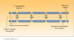
Another aspect of serially illuminating the detectors is that each successive detector receives less optical power than the preceding one. Thus saturation characteristics are influenced most by the first detector. To achieve uniform illumination and hence higher saturation power, a variation on the VMDP has been proposed in which the optical signal is split evenly n ways before illuminating the n detectors.5 Adjusting the optical path delays allows in-phase combining of the electrical signals.
Overall, much research is being carried out to improve the performance of high-speed photodetectors. The RCE detector sidesteps the speed/efficiency trade-off by placing the absorbing region within a Fabry-Perot cavity. And these detectors are now being fabricated for use at the important communication wavelengths. Distributed detectors, which include the VMDP, are solving the problem of detecting the high-speed, high-power optical signals needed for low-noise, high-dynamic-range, analog fiber-based systems.
REFERENCES
1. M. S. Ünlü and S. J. Strite, J. Appl. Phys. 78, 607 (1995).
2. S. S. Murtaza et al., Appl. Phys. Lett. 69, 2462 (1996).
3. A. G. Dentai et al., Electron. Lett. 27, 2125 (1991).
4. L. Y. Lin et al., IEEE Photon. Technol. Lett. 8, 1376 (1996).
5. C. L. Goldsmith et al., IEEE Photon. Technol. Lett. 9, 988 (1997).
About the Author
Andrew Davidson
Senior Staff Engineer, MKS Newport - New Focus
Andrew Davidson is a Senior Staff Engineer at MKS Newport - New Focus (Irvine, CA).
Robert Marsland
VP, High Speed Data Group, MKS Newport - New Focus
Robert Marsland was VP, High Speed Data Group at MKS Newport - New Focus from 1990 through 2003.