Single-photon Detection: NbN superconducting nanowire detector resolves photon numbers up to 24
In between the few-hundred-photons-and-above detection regime, where conventional linear detectors such as indium gallium arsenide (InGaAs) photodiodes reign, and the single-photon regime targeted heavily by numerous types of detectors, is the single- to hundred-photon regime. This regime needs a linear photodetector—a photon-number-resolving detector (PNRD)—for purposes such as near-infrared (NIR) spectroscopy, optical quantum computing, and communications.
Because most single-photon detectors produce an output signal that is independent of the number of photons above 1 because of their nonlinear internal amplification method, they are not suitable for this regime. A type of sensor called a transition-edge sensor, which requires elaborate cryogenic cooling to temperatures of less than about 100 mK, have a linear photon response up to on the order of 10–20 photons. However, in addition to the expensive cooling, transition-edge sensors have a maximum frequency of less than 1 MHz.
Researchers from the Istituto di Fotonica e Nanotecnologie (IFN), CNR (Rome, Italy), and the COBRA Research Institute, Eindhoven University of Technology (Eindhoven, Netherlands) have created an alternative that can resolve up to 25 distinct output levels corresponding to the detection of n = 0 to n = 24 photons, and can do this at frequencies up to several hundred megahertz.1 In addition, it operates at 1.6 K, which—although low—is much easier to achieve than 100 mK.
Niobium nitride superconducting detector
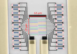
The 24-pixel device is based on niobium nitride (NbN) superconducting nanowires in a series configuration (see figure). Voltage pulses generated by the pixels are summed up into a single readout pulse that has a height proportional to the detected photon number. The device is intended to accept NIR light from an optical fiber.
A 4-nm-thick layer of NbN is deposited on a quarter-wave silicon dioxide (SiO2) optical cavity on top of a silicon substrate—a process that includes reactive-ion etching to produce 100-nm-wide nanowires that are folded into meandering paths in each 1 × 6 μm pixel with a 40% fill factor.
Light at a 1310 nm wavelength from a pulsed laser diode was used to test the detector—a fiber-based beamsplitter and variable attenuator brought the light level down to the required single- to few-photon regime. A low-pass electrical filter was added to the amplification chain to improve the visibility of the voltage peaks of the detector.
When no light is hitting the detector, all nanowires are in the superconducting state, with current flowing through the nanowires. If a photon strikes a pixel, that pixel has a temporary disruption in its superconductivity that produces a resistance for that pixel, which is sensed. Two photons simultaneously striking two pixels are sensed as a resistance twice as high as that when a single photon strikes a single pixel.
The detector's output pulses (measured with a 40 GHz oscilloscope) had a jitter of 116 ps and a 1/e decay time of 13 ns, which is a much faster response time than those for transition-edge-sensors and silicon photomultipliers with upconversion. The detector's response to square-wave and sinusoidal signals was measured-the maximum modulation frequency was about 700 MHz.
"The next step in our research will be the optimization of the NbN deposition (the absorbing superconducting film) and of the fabrication process in order to increase the detector's quantum efficiency," says Francesco Mattioli, one of the IFN researchers. "The detector in the article is a proof of principle and a high quantum efficiency is absolutely necessary for a real application (for example, deep-space communications or quantum information processing in general). The second step could be the increase of the dynamic range to at least a 48-pixel range."
REFERENCE
1. F. Mattioli et al., Opt. Express, doi:10.1364/oe.24.009067 (Apr. 18, 2016).
About the Author
John Wallace
Senior Technical Editor (1998-2022)
John Wallace was with Laser Focus World for nearly 25 years, retiring in late June 2022. He obtained a bachelor's degree in mechanical engineering and physics at Rutgers University and a master's in optical engineering at the University of Rochester. Before becoming an editor, John worked as an engineer at RCA, Exxon, Eastman Kodak, and GCA Corporation.

