Diffraction mask design brings 3D imaging to standard CMOS image sensors
GIL SUMMY and JAMES MIHAYCHUK
3D imaging is an essential part of many human and machine vision applications in security, consumer electronics, automotive, and many other industries; because it is so widely used, any savings in hardware, size, and computational load is a benefit. This article provides an overview of DEPTHIQ, a 3D computer-vision approach developed by AIRY3D (Montreal, QC, Canada) that is a simpler and more-affordable alternative to traditional 3D imaging technologies, and enables faster, cheaper, and smaller 3D vision systems.
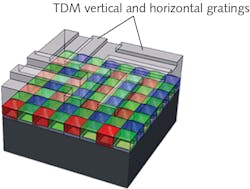
The DEPTHIQ technology places an optical encoding transmissive diffraction mask (TDM) on a standard CMOS image sensor to generate both high-quality 2D color images and near-field depth maps that are inherently correlated.
The addition of two thin layers of transmissive material, collectively making the TDM, over the top of most CMOS image sensors can provide 3D sensing capabilities with virtually no reduction in 2D image quality. These layers use the process of diffraction from a phase grating to realize compact, low-cost, low-compute solutions for 3D image capture.
Figure 1 shows how the transparent TDM is applied to a conventional CMOS image sensor. Briefly, a clear material forms a diffraction grating over the microlens array. This has a minimal impact on both the properties of the microlenses and the color filter array (CFA). Through refraction and filtering of light before it reaches the pixel photodiodes in the active silicon, the microlenses and CFA strongly influence the spectral response and color accuracy. The TDM design is optimized to be compatible with these essential micro-optical structures of the original 2D CMOS image sensor.
TDM design overview
The physics underlying the TDM is diffraction from a phase grating. Thus, the TDM is a transparent structure rather than a lossy mask and does not rely on opaque, lithographically patterned features. As such, a TDM can be added to any existing image-sensor design through a small number of postprocessing steps.
Because it is typically only a few microns thick, a TDM can normally be added to an image sensor without requiring changes to the lens or other camera-module components. However, as with any image sensor, it remains important to select a compatible lens in terms of numerical aperture (NA), chief-ray angle (CRA), and alignment tolerancing.
Through the process of diffraction, the TDM is designed to encode phase/direction information into the light intensity distribution. This normally “hidden” degree of freedom contains information about the depth of the light-emitting source. The directional information is extracted by the TDM using a process based on the near-field optics phenomenon of Fresnel diffraction. Specifically, the light field generated by a periodic structure such as a diffraction grating is described by the self-imaging phenomenon known as the Talbot effect. This is a phenomenon in which both the phase and intensity of the light form fractal-like diffraction patterns in the vicinity of the grating.
Optical-design considerations
The design of the TDM and its camera module will be determined not only by the 2D imaging requirements, but also by 3D specifications such as the desired depth-detection range and the relative depth accuracy. The depth accuracy is usually expressed as a percentage error relative to the known ground-truth distance to the target object. For example, a well-known commercially available stereo camera claims a useful range from about 20 cm to several meters and absolute error not more than 2%.
Practical performance will depend on the intended use of a 3D imaging solution and details of the deployment in terms of lighting and contrast. Nevertheless, it is possible to tentatively specify a 3D imaging system, whether TDM-based or otherwise, through a combination of 2D image-capture specifications and the desired depth range and accuracy.
The optical designer must also demonstrate the ability to easily reconstruct a high-quality 2D image from the image sensor with the TDM in place. Key measures of image quality to be evaluated include the modulation transfer function (MTF), quantum efficiency (QE), color fidelity, and photoresponse nonuniformity (PRNU, or the “lights on” counterpart to fixed pattern noise).
Numerical aperture (NA)
For a 2D image sensor, important design parameters include the NA, the CRA, and the desired 2D resolution (number of pixels). For an image sensor that is extended to 3D imaging using a TDM, these attributes are no less important, although these optical properties must also be assessed for their impact on the depth resolution and accuracy.
The NA is approximately the product of the index of refraction and the maximum half-angle for a marginal ray of the light cone for light accepted by the camera lens. That is, the NA describes the angular range in which the system admits light.
For light admitted by the objective lens that falls within the cone defined by the marginal rays, an appropriately designed TDM should be capable of providing useful directional information in the grating-modulated 2D image, without contributing distortion to either the 2D or 3D image data.
Chief-ray angle
The chief-ray angle (CRA) is defined as the angle between the normal to the first surface of the pixel-array active silicon and a ray of light that passes through the center of a particular microlens.
The CRA varies from the center of the pixel array to its corners or edges. To correct for lens shading (vignetting) effects in pixels nearer to the edge of the pixel array, the center of each microlens is shifted relative to the center of the corresponding photodiode in the active silicon (see Fig. 2). Near the center of the array, the CRA is zero so that most light rays are assumed to reach the pixels as paraxial rays. For sensors with a non-zero CRA, the CRA of the microlens array is still zero for pixels at the center of the array. However, due to intentional shifting of microlenses relative to the corresponding pixel photodiodes, the microlens CRA will typically increase in magnitude for pixels along a line from the center to the corner of the array.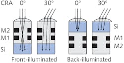
In Figure 2, M1 and M2 designate opaque metal layers and Si indicates the active silicon of the pixel photodiode. As shown on the right in Figure 2, a back-illuminated pixel structure will generally have a thinner optical stack. For similar optical properties for the microlens array, a back-illuminated pixel’s short optical stack is more compatible with a higher CRA.
The TDM should be optimized to account for the microlens shifts as well as any CRA mismatch between the lens and the pixel array. To this end, designers may choose to develop a specific design based upon a maintaining the optical phase shift within a specified fraction of the period of the TDM grating.
A combination of macroscopic and pixel-level optical-design parameters must be considered in order to optimize a TDM-based 3D sensor design to ensure useful operation throughout the desired depth range. The angular sensitivity is linked not only to the TDM features, but also to the NA of the lens.
TDM grating design parameters
A number of primary TDM geometrical design parameters can be defined (see Fig. 3). These geometrical features can be varied appropriately in order to optimize the depth accuracy and 2D image quality.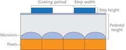
Grating materials. The TDM grating material must be transparent in the desired wavelength range. The pedestal and grating materials must also be compatible with reliable wafer-level postprocessing of conventional CMOS image sensors. In addition to being mechanically compatible with the microlens array, the TDM must have a sufficient difference in the index of refraction between the pedestal (low index) and the microlenses (high index) in order to maintain the intended focusing effect of each microlens.
Grating period. Ideally, the TDM grating period (pitch) should be tuned specifically for compatibility with the optical stack present in a particular pixel structure. The TDM optical design should minimize pixel-to-pixel crosstalk while maintaining the desired angular response. The grating period also influences the depth sampling rate (filling ratio) for object depth determination. Typical grating periods are small multiples of the pixel pitch.
Grating step height. The TDM grating step height is tuned in concert with the height of the pedestal. A wide range in step heights is possible, depending on the pedestal height and optical properties.
Grating phase shift. The TDM grating phase shift is defined by the lateral offset between a particular grating step and the center of the photodiode in the corresponding pixel. A grating peak that is situated directly above the center of the pixel has no grating phase shift. A grating peak situated directly over an imaginary line of symmetry separating a pixel photodiode from its nearest neighboring photodiode would have a phase shift of 90° (see Fig. 3).
Pedestal thickness. The pedestal thickness is measured from the base of the microlens array to the base of the TDM grating steps. The optical path through the pedestal affects the modulation depth as well as the angular sensitivity of a particular TDM design. Typically, the pedestal is several microns thick. While a higher-index pedestal could be made thinner, as already mentioned, the pedestal cannot be index-matched to the microlens material if the microlenses are to be effective.
Grating direction. The TDM grating direction refers to the orientation of the ruling of the grating relative to the horizontal rows or vertical columns of the pixel array. The orientation of the grating determines the row- or column-wise direction in which diffraction modulates the light-generated signals whenever photoelectrons are generated in the photodiodes of the pixel array. Since diffraction mostly occurs along the short axis of the grating, a vertically or horizontally ruled grating can detect depth only at contrast edges in a scene that have the same orientation as themselves.
Careful design and optimization of the TDM based on material, optical, and geometrical factors serve to improve the 3D image-acquisition capabilities. A complete model would consider the camera lens, the monolithically integrated TDM grating, and the optical design of the pixels of the CMOS image sensor. The TDM composition and grating profile, the grating phase shift relative to the pixel array, and the pedestal thickness can all be used to tune the modulation depth and angular sensitivity available for depth computation.
To date, these TDM design approaches have been successfully applied to implement single-sensor 3D imaging solutions based on a wide range of CMOS image sensors. The TDM approach has been adapted to both backside-illuminated mobile sensors for smartphones and frontside-illuminated, global-shutter machine-vision sensors. As such, TDM structures have been incorporated onto sensors having pixel pitches from about 1 to 3 µm and pixel counts from about 2 to 20 Mpixels.
AIRY3D is working to enable complete 3D systems through efficient depth computation algorithms and integration with various embedded vision platforms. DEPTHIQ TDM-based single-sensor designs show a strong potential for rapid integration into single-aperture cameras in mobile, security, robotics, and automotive systems.
Gil Summy is Director, Optics Group and James Mihaychuk is Product Manager, both at AIRY3D, Montreal, QC, Canada; e-mails: [email protected] and [email protected]; airy3d.com.