OPTICAL DESIGN/LASER-TISSUE INTERACTION/BIOIMAGING: A detailed look at microoptics for biomedicine
Microoptics play a critical role in improving biomedical applications—and are now enabling new advances in life sciences. Systems designers must understand their operation and application to leverage the advantages they offer.
ByMarc D. Himel and Tim Lindsey
The combination of microoptics with lasers and now CMOS sensors has done more than improve existing biomedical applications: It is opening the door to entirely new areas, from R&D to point-of-care. With the increasing use of lasers and image sensors, and the desire to reduce sizes and costs to allow for more point-of-care systems, the application of microoptics in healthcare is destined to grow. Let's take a look, from a systems-design perspective, at considerations relevant to microoptics—considerations that today make all the difference on both the source and imaging sides of an optical system for applications such as vision correction, skin rejuvenation, robotic surgery, and more.
One of the more mature applications of microoptics to biomedicine is in the area of laser-assisted in situ keratomileusis (LASIK), where a 193 nm excimer laser is used to sculpt the cornea to correct vision problems such as hyperopia, myopia, and astigmatism. Most excimer lasers have an elliptical-shaped output that is roughly top hat-shaped in one direction and Gaussian in the other, with non-uniformity of 25% or more. If this raw beam were used to ablate the cornea, the cure would be worse than the disorder! With the appropriate application of diffractive optics, however, such a beam takes on a smooth Gaussian profile ideal for raster scanning across the eye; the result is effective treatment for millions of people worldwide (see sidebar, online at www.bioopticsworld.com/himel/sidebar.html). Meanwhile, let's take a look at two other examples of microoptics' utility for biomedicine.
Beam control for skin treatment
Recent progress in infrared microoptics now plays an important role for fractional photothermolysis, a resurfacing treatment for scarring and other skin conditions.1 This procedure uses CO2 (10.6 μm wavelength) or Er:YAG (2.94 μm) laser energy in small spots called micro thermal zones that penetrate the dermis to target the skin's deeper layers. Treating small spots surrounded by unexposed tissue allows treatment areas to heal in days rather than weeks or even months, as is standard with traditional treatment of large surface areas.
The key to successful design of a selective micro photothermolysis laser system is controlling both the spot size on the skin and the waist location in the optical setup. Diffractive and refractive microoptics that use the proper design and material, in combination with more traditional optics, are necessary to achieve this goal. For such a system to meet all the requirements, it is best to take a whole-system approach to design rather than break design requirements into sub-modules. In this way, individual fabrication and performance variations can be dealt with more effectively.
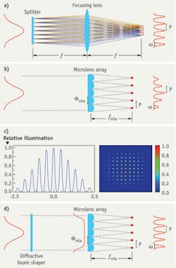
The first option for creating spots on the skin is the use of diffractive beamsplitters, which make design and layout of the optical system quite easy (see Fig. 1a). In this configuration, the spots will be focused in telecentric image space. The spot-to-spot distance, known as pitch, is determined by the diffraction angle and the focal length of the focusing lens. This equation is as follows:
P = ƒ × tan(θd)
P - pitch, distance between spots at skin
ƒ - focal length of Fourier lens
θd - diffraction angle
In this layout, you can get different spot sizes and pitches by simply varying the focal length of the Fourier lens. However, this 2ƒ layout requires a longer optical path and a high-quality aspheric focusing lens (without an aspheric lens, spot sizes will vary in diameter because of spherical and off-axis aberrations).
An alternative method for creating an array of spots is the use of a refractive microlens array (MLA). By using an MLA with a collimated input, spots will be created by individual lenslets (see Fig. 1b). An MLA-based system allows the spots to be focused to a shorter distance onto the skin, so the entire system is much more compact. With this setup, however, spot size is now determined by the lenslet aperture described in the equation below, rather than the input beam diameter, assuming a square lenslet shape. Pitch is determined by pitch of the microlens array and spot size is:
ω = 2 × λ × (ƒmla)/ (Φmla)
where ω = spot size on the skin; λ = laser wavelength; ƒmla = focal length of lenslet; and Φmla = aperture of a single lenslet of the MLA.
In many cases, the input beam is a single-mode beam with Gaussian intensity distribution. As a result, the final spot array will show a Gaussian rolloff across the illuminated skin (see Fig. 1c). Eliminating this is optimally done by illuminating the MLA with a uniform intensity profile. This can be accomplished by using a source such as a multimode fiber laser or a fiber-delivered high order mode, or by adding flat-top, beam-shaping optics prior to the microlens array. In this case, the microlens array is illuminated with a top-hat beam profile, resulting in uniform intensity of the spots on the skin. An optical setup for this is shown below in Figure 1d. In the case of the ablative laser procedures, power and wavelength are of particular interest. Materials have specific transmission characteristics depending on the wavelength. High-performance microoptics materials are silicon (absorbing at 10.6 μm) and fused silica (absorbing at 2.94 μm). So, other materials such as zinc selenide (ZnSe) and sapphire are preferred at these wavelengths.
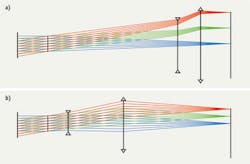
We can add some adjustability to the output pattern by incorporating a ZnSe zoom lens that reimages the focal plane of the microoptic. A simple two-position zoom system design at λ = 2.94 μm changes the spacing between the spots by a factor of two while maintaining the location of the final image plane (see Fig. 2). This design is also telecentric in image space so that the spacing of the spots does not change with defocus. Further adjustability could be added such as a continuous zoom or exchangeable microoptics to change the output pattern.
Perfect for plenoptics
Besides their utility for light shaping on the source side of an optical system, microoptics are also useful on the imaging side. For instance, plenoptic (or light-field) imaging was invented over a century ago, but could not be effectively realized because the required microlens arrays, high-resolution CMOS sensors, and high-speed video processing was not available.2 Recent advances in all these areas are finally enabling the technique. Plenoptic imaging provides a means to generate a three-dimensional (3D) depth map from a single camera and objective lens. The resulting data can be used to create 3D images or video, measure distance, refocus an image after the fact, extend and adjust the depth of field, or shift perspective. It has already found application in volumetric velocimetry, astronomy, and consumer cameras.3-6 It is only a matter of time before we see this technology deployed to generate real-time 3D video in endoscopy and minimally invasive surgery and to extend the depth of field or refocus images after the fact in real-time microscopy of live biological samples.
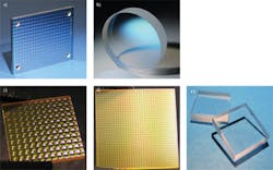
Critical to these advanced applications are the quality of the microlens array (MLA) and its assembly to the CMOS sensor. Among factors to consider for the MLA is the material. For endoscopy, where the sensor is integral to the endoscope, the system must survive sterilization, and thus an all-glass or fused-silica MLA may be required rather than plastic or polymer-on-glass. Although most current applications are in the visible range, microlens arrays can be manufactured from various materials that cover the wavelength range from deep ultraviolet (DUV) to thermal infrared (IR). Different etch techniques and chemistries allow us to manufacture microoptics in calcium fluoride (CaF2) for DUV, fused silica and other glasses for the visible, or in sapphire, germanium (Ge), silicon (Si), and ZnSe for IR applications (see Fig. 3).
Once the appropriate material has been chosen, the MLA can be designed for a specific plenoptic application. The typical parameters we can control are the lens pitch, radius of curvature, conic constant, lens shape, and fill factor. In most embodiments of a plenoptic camera, the MLA can have circular or full-fill-factor lenses, but there are advantages to using a full-fill-factor array. With circular lenses on a square or hexagonal grid, light will pass through the area without the lenses unless an aperture is used to block this stray light. Using our lithography processes, it is easy to align and pattern an absorptive metal coating for very high-volume and low-cost applications. Where molded optics are needed, however, aligning and patterning this metal layer is quite complex and probably will not be appropriate. A full-fill-factor lens array is a better solution, as no metal aperture layer is required. Jenoptik's grayscale lithography enables manufacture of these full-fill-factor lens arrays while maintaining the correct lens shape into the corners and thus minimizing aberrations.
The key to enabling high performance is fabricating and assembling the MLA to the CMOS sensor with enough precision to ensure high-quality performance of the system. This can be better understood by looking at an example. Suppose we have a 12 Mpixel sensor with 9.0 μm-sized pixels and a lens array with a 63 μm pitch. Most CMOS sensors include a 300-μm-thick cover glass to protect the active sensor surface from damage or dust particles. So, the shortest lens effective focal length (EFL) will be about 500 μm. In this case, the MLA will have an f/# of 8. The geometric depth of focus, defined by 2*λ*(f/#)2, is approximately 70 μm for visible light. At first glance, this looks reasonable from a fabrication and assembly perspective. But let's take a look at some of the tolerances:
Cover glass thickness variation is typically ±30 μm for inexpensive float glass.
Lens array focal length variation is typically between 1 and 3%, depending on the fabrication process. A 3% variation for our 500 μm EFL lens is ±15 μm.
The MLA needs to be separated from the cover glass with a 200 μm spacer. Let's assume we can control this spacer to ±20 μm.
The root-mean-square (RMS) error associated with these three tolerances is about 40 μm, or over half of our error budget. There is one more important tolerance to consider, though: The tilt of the lens array with respect to the CMOS sensor. Assuming the sensor is 36 mm long, we would need to maintain tilt to <30 μm across the entire MLA. Current measurement and advanced packaging methods allow this to be done economically for high-performance applications, but it could be difficult to achieve for some of the lower cost and higher volume applications.
The f/8 system described above may be either light-starved in practical use or it may not match the f/# of the imaging lens for the specific application. In this case we may need to use a CMOS sensor with the cover glass removed, thus allowing us to decrease the f/# of the MLA while maintaining the same pitch. For an f/2 system, the MLA will have an EFL of 125 μm and a DoF of ~5.0 μm. Maintaining the 3% tolerance on EFL yields a variation of 3.75 μm or most of our allowed tolerance—which implies significant challenge to assembly of the lens to the sensor. This can be accomplished by performing exacting metrology on the MLA to precisely measure the lens EFL and accounting for this when we specify the spacer used to separate the MLA from the CMOS sensor. Precision CNC machining, perhaps in combination with glass microsphere-filled adhesives, will allow us to meet these challenges effectively.
In some applications it may not be beneficial to attach the MLA directly to the CMOS sensor, but to reimage it with a telecentric 1X relay lens.7 This could allow a plenoptic lens to be inserted into existing hardware systems, avoiding the need to upgrade an expensive camera. This, of course, adds complexity to the alignment of the system, as we now need to account for these additional tolerances:
1. The distance between the sensor surface and the lens mounting flange;
2. The back focal length variation of our 1X relay lens; and
3. Thermal expansion effects.
These are straightforward to deal with if each plenoptic module is aligned to a specific camera module, but if we want to be able to use one plenoptic module with multiple cameras, we will need to have hardware and software that allows for the adjustment and calibration of the system. We can add one or two focus mechanisms as a first step, as this will allow us to focus the objective lens to the MLA and the MLA to the sensor. If our relay lens is telecentric, we should not see too much change in magnification through focus, thus minimizing the complexity of any calibration requirements. Clearly, a full system-level approach to design will reveal the most optimum and cost-effective solution.
More and more microoptics
The continued development of new applications that use laser sources or advanced CMOS sensors, the need for microoptics to add additional functionality, miniaturization, and cost reduction will only increase. Further, advances in precision CNC machining, microoptics fabrication, and packaging will likely increase the presence of microoptics, as they will allow such designs to be incorporated into point-of-care and portable health care modules and systems.
In fact, the next wave of advancements in microoptics may not be the microoptics themselves, but the way they are seamlessly integrated with electronics, micro-electromechanical systems (MEMS), and other devices into small modules for cost-effective solutions to what seem like intractable problems today. So, we may see microoptics play an important role in mapping DNA and proteins; small-form-factor, field-usable microscopes; digital holographic microscopes; micro-sized endoscopes, point-of-care melanoma and vision screening; microfluidic lab-on-a-chip imaging; and biometric sensing.
REFERENCES
1. G. Geronemus, Lasers Surg. Med., 38, 3, 169–176 (March 2006).
2. G. Lippmann, Comptes Rendus de l'Académie des Sciences, 146, 9, 446–451 (March 1908).
3. C. Perwass and L. Wietzke, Proc. SPIE, 8291, 829108 (2012).
4. T. Nonn, J. Kitzhofer, D. Hess, and Ch. Brücker, 16th International Symposium on Applications of Laser Techniques to Fluid Mechanics, Lisbon, Portugal (July 9–12, 2012).
5.L. F. Rodríguez-Ramos et al. Proc. SPIE, 8384, 83840D-83840D-9 (2012).
6. www.lytro.com
7. J.H. Steurer, M. Pesch, and C. Hahne, Proc. SPIE, 8291, 829109-1-829109-9 (2012).
Marc D. Himel, Ph.D., is Business Development Manager for Microoptics at Jenoptik Optical Systems GmbH (Jena, Germany), and Tim Lindsey is Sales Manager for Microoptics at Jenoptik Optical Systems Inc. (Huntsville, AL); www.jenoptik.com/microoptics. Contact Dr. Himel at [email protected].


